Superconducting-qubit lithography (Al/AlOx/Al junctions, Nb wiring, 300 mm) fab_sc
300 mm junction lithography and post-fabrication frequency trimming (laser annealing, ABAA) set the frequency spread every superconducting architecture inherits.
Superconducting-qubit lithography (Al/AlOx/Al junctions, Nb wiring, 300 mm)
IBM Albany 300 mm / Anderon foundry; Google Santa Barbara; Rigetti ABAA trimming (97.4% frequency-targeting success); OQC 500-qubit wafer-scale package.
Brief →Key references
Design space — attributes
- (a) carrier affinity
- fabricated
- (b) time · entangling
- —
- (c) readout
- —
- (d) mobility
- —
- (e) control
- —
- (f) error structure
- coherent / calibration
- (g) manufacturing
- superconducting lithography
Evaluation space — dated attributes
The OQC package is on 3-inch sapphire; its abstract rounds median T1 and T2e together to ~100 µs, while the body reports T1 97 µs and T2e 129 µs separately; it is a packaging result, not a processor.
Standard records
Actors & goals — annotations
Edges
Used by 97 machines (93 primary · 4 alternate)
- superconducting circuits 93
- Academia Sinica 20-qubit superconducting quantum computer Academia Sinica press ▨ 🔎
- Alice & Bob Boson 4 Alice & Bob press ▤ Fig. 2B (optical micrograph: fractal capacitor, 29-junction chain, ATS, quarter-wavelength coplanar filter); App. A1 (tantalum patterning on sapphire; Dolan-bridge Al junctions) ✅
- Alice & Bob Graphene Alice & Bob press ▣ Fig. 9 (flip-chip two-layer layout) ✅
- Alice & Bob Helium (on-premise system) Alice & Bob whitepaper press ▥ §The Hardware Behind Cat Qubits (sapphire chips with printed superconducting circuits; Ta/Al resonator); §MILESTONE 1 Challenge 1: Herd the Cats (nanofabrication) ✅
- Alice & Bob Helium 2 ("Galvanic Cat") Alice & Bob press ◌ 🔎
- IBM Quantum System Two at Amaravati Quantum Valley Tech Park IBM with TCS and the Government of Andhra Pradesh ◌ 🔎
- Anyon MonarQ Anyon Systems product page press ◌ 🔎
- AWS dual-rail transmon erasure line AWS Center for Quantum Computing (named Amazon Center for Quantum Computing in the Apr 2026 paper) paper ▤ App. A (Device) 🔎
- AWS Ocelot AWS Center for Quantum Computing ▤ App. A (Device fabrication) ✅
- Baihua (Quafu platform) Beijing Academy of Quantum Information Sciences paper ◌ 🔎
- Dongling (Quafu platform) Beijing Academy of Quantum Information Sciences ◌ 🔎
- Haituo (Quafu platform) Beijing Academy of Quantum Information Sciences ◌ 🔎
- ScQ-136 "Baiwang" Beijing Academy of Quantum Information Sciences ◌ 🔎
- Shenglian (BAQIS) Beijing Academy of Quantum Information Sciences paper ◌ 🔎
- IBM Quantum System Two, Donostia-San Sebastian Basque Government (BasQ) - IBM-Euskadi Quantum Computational Center press ◌ 🔎
- Quantum Spain quantum computer at BSC Barcelona Supercomputing Center (Quantum Spain; installed by Qilimanjaro-GMV) press ◌ 🔎
- WACQT quantum computer (Chalmers 25-qubit flip-chip processor) Chalmers University of Technology (WACQT) ◌ 🔎
- Tianyan-176 / Tianyan-176 II (and Tianyan-24 sibling) China Telecom Quantum Group + QuantumCTek paper paper paper ◌ 🔎
- Tianyan-287 China Telecom Quantum Group / QuantumCTek / CAS paper docs docs ◌ 🔎
- Tianyan-504 / "Xiaohong" chip China Telecom Quantum Group + CAS + QuantumCTek paper docs docs ◌ 🔎
- 6-qubit superconducting quantum processor DRDO DYSL-QT with TIFR and TCS ▨ ✅
- Surface-17 ETH Zurich (Quantum Device Lab) paper paper ▤ Appendix A ✅
- IBM Quantum System One, Ehningen Fraunhofer-Gesellschaft ◌ 🔎
- Fujitsu >10,000 physical / ~250 logical (STAR) Fujitsu + AIST + RIKEN press ▨ 🔎
- Fujitsu 1,000-qubit machine Fujitsu (+ RIKEN) link ◌ 🔎
- Sycamore Google Quantum AI paper ▤ §Building a high-fidelity processor (Al metallization + JJs, indium bump-bonds); SI §II Fabrication and layout ✅
- Sycamore-class 72-qubit processor Google Quantum AI paper paper ◌ 🔎
- Willow Google Quantum AI paper paper product page ▤ ✅
- IBM Quantum Blue Jay IBM blog ◌ 🔎
- IBM Quantum Cockatoo IBM press ◌ 🔎
- IBM Quantum Condor IBM blog press ▥ §Breaking the 1,000-qubit barrier with Condor (50% qubit density, qubit fabrication + laminate size advances) ✅
- IBM Quantum Eagle r1-r3 IBM paper paper paper ▤ §III.5 (Eagle) ✅
- IBM Quantum Egret IBM docs ◌ 🔎
- IBM Quantum Falcon r5.11 IBM paper blog ◌ 🔎
- IBM Quantum Flamingo (l-coupler proof of concept) IBM blog ◌ 🔎
- IBM Quantum Heron r1 IBM paper blog press ◌ 🔎
- IBM Quantum Heron r2 IBM paper paper press ◌ 🔎
- IBM Quantum Heron r3 (ibm_pittsburgh) IBM blog press ◌ 🔎
- IBM Quantum Kookaburra IBM docs ◌ 🔎
- IBM Quantum Loon IBM blog ▥ Fig. ('IBM researcher holding a 300mm IBM Quantum Loon wafer'); §Building our fault-tolerant architecture ✅
- IBM Quantum Nighthawk r1 IBM docs blog blog ▥ §New capabilities for scaling advantage (all chips start on 300 mm wafers, Albany NanoTech; 2x R&D speed, 10x complexity) 🔎
- IBM Quantum Nighthawk r2 IBM blog ▨ 🔎
- IBM Quantum Osprey IBM blog press ◌ 🔎
- IBM Quantum Starling IBM blog ◌ 🔎
- IBM Quantum System Two at CSCS (Swiss Quantum Innovation Hub) IBM with ETH Zurich (CSCS) and Lockheed Martin press ▨ fabrication paragraph (300 mm wafer facility, Albany NanoTech Complex) ✅
- IQCC superconducting facility Israeli Quantum Computing Center (Quantum Machines + QuantWare + Qolab + ORCA) product page product page press ◌ 🔎
- IQM Emerald (IQM Crystal 54) IQM Quantum Computers blog ◌ 🔎
- IQM Garnet (IQM Crystal 20) IQM Quantum Computers paper ▤ §2.5 Control routing and fabrication ✅
- IQM Halocene IQM Quantum Computers press press link ◌ 🔎
- IQM Spark at Eldorado Research Institute IQM Quantum Computers with Instituto de Pesquisas Eldorado press ▦ features (IQM-owned production facilities and clean room) ✅
- IQM Star 24 IQM Quantum Computers link ◌ 🔎
- IQM six-qubit star QPU (Deneb-class) IQM Quantum Computers paper paper docs ◌ 🔎
- VLQ IT4Innovations National Supercomputing Center (VSB - Technical University of Ostrava) press ◌ 🔎
- KRISS domestic superconducting QPU Korea Research Institute of Standards and Science press press ◌ 🔎
- KRISS 50-qubit-class superconducting system Korea Research Institute of Standards and Science press ◌ 🔎
- Advanced Quantum Testbed (AQT) Lawrence Berkeley National Laboratory ◌ 🔎
- OQC ATHENA Oxford Quantum Circuits product page ▥ ATHENA card ✅
- OQC ATLAS Oxford Quantum Circuits product page ▥ ATLAS card ✅
- OQC GENESIS Oxford Quantum Circuits product page product page press ▤ §II (device and resonator on opposite sides of substrate; methods per ref. [43]) ✅
- OQC TITAN Oxford Quantum Circuits product page ▥ TITAN card ('100 mm') ✅
- OQC Toshiko Oxford Quantum Circuits product page ▤ §IX Materials and Methods (enclosure CNC-machined 6061 Al; SPC UT47 coax out-of-plane wiring) ✅
- Origin Wukong 102 Origin Quantum ◌ 🔎
- Origin Wukong-180 (4th gen) Origin Quantum press ◌ 🔎
- Origin Wukong (3rd gen) Origin Quantum paper ◌ 🔎
- Qolab devices at the IQCC Qolab ▦ §Window-junction process; SEM figure (a) tilted-angle SEM of the window junction, (b) magnified junction ✅
- QpiAI Indus QpiAI press ◌ 🔎
- QpiAI Kaveri QpiAI press ▨ 🔎
- QuantWare Contralto-A17 QuantWare press ▨ ✅
- QuantWare Tenor-D64 QuantWare product page ▨ ✅
- QuantWare Bass-A10K (VIO-40K) QuantWare press ▦ §VIO-40K announcement (Kilofab, Delft, opens 2026, 20× capacity) ✅
- Rigetti Ankaa-2 Rigetti Computing paper paper ◌ 🔎
- Rigetti Ankaa-3 Rigetti Computing blog press press ◌ 🔎
- Rigetti Cepheus-1-108Q Rigetti Computing blog ▤ §II.C Fabrication (qubit chips by standard lithography on high-resistivity Si; indium bump bonding to carrier) ✅
- Rigetti Cepheus-1-36Q Rigetti Computing blog press ▤ §II.C Fabrication (qubit chips by standard lithography on high-resistivity Si; indium bump bonding to carrier) ✅
- Rigetti Novera Rigetti Computing product page press ▦ 'designed and manufactured in-house at Fab-1' ✅
- RIKEN 64-qubit superconducting processor RIKEN with AIST, NICT, Osaka University, Fujitsu, NTT press press ◌ 🔎
- RIKEN-Fujitsu 256-qubit superconducting quantum computer RIKEN RQC + Fujitsu press press ◌ 🔎
- RIKEN RQC-Fujitsu 64-qubit superconducting quantum computer RIKEN RQC + Fujitsu press ◌ 🔎
- SEEQC SFQ-controlled 5-qubit system SEEQC paper press ▤ Supp. §A Device Design and Fabrication (SEEQC SFQuClass Nb process, 1 kA/cm2 JJs, high-kinetic-inductance layer) ✅
- SpinQ Ursa Major (25 q / 103 q) SpinQ Technology product page press press ◌ 🔎
- SUSTech four-dual-rail-qubit processor Southern University of Science and Technology (Huang et al.) paper paper ▣ Fig. 1a; Supplementary §I ✅
- Toshiba double-transmon coupler Toshiba + RIKEN RQC + University of Tokyo paper press ▤ Appendix A: Fabrication ✅
- Kunlun Tsinghua University IIIS (D.-L. Deng) with Zhejiang University (H. Wang, C. Song groups) paper paper ▣ Fig. 1a right (magnified coupler crossing microstructure); SI: Multi-length couplers ✅
- Zuchongzhi 2.1 USTC / Hefei National Laboratory paper ▣ Fig. 1a (two sapphire chips combined by flip-chip technique) ✅
- Zuchongzhi 3.0 USTC / Hefei National Laboratory paper paper press ▤ §II (fabrication procedure) ✅
- Zuchongzhi 3.2 USTC / Hefei National Laboratory ◌ 🔎
- VTT Q50 VTT Technical Research Centre of Finland product page ▨ 🔎
- Zhuangzi 2.0 (Chuang-tzu 2.0) CAS / Peking University paper paper press ▤ §S3.A Device fabrication ✅
- Zhejiang University 125-qubit surface-code processor Zhejiang University + Graduate School of China Academy of Engineering Physics (Beijing) paper ◌ 🔎
- D-Wave gate-model dual-rail system D-Wave Quantum press ◌ Fig. 1a (three SQUID transmon couplers; transmon and readout resonator per cavity) 🔎 (alternate)
- Nord Quantique single-mode GKP Nord Quantique paper press ◌ 🔎 (alternate)
- Nord Quantique Tesseract Nord Quantique product page press ▤ §II.1 Experimental setup / App. A.1 Experimental device ✅ (alternate)
- Aqumen Seeker Quantum Circuits Inc. (acquired by D-Wave, Jan 2026) press ◌ 🔎 (alternate)
- quantum annealers 4
- Advantage D-Wave Quantum docs ▣ §III.D Minimizing Φ-DAC footprint (6 Nb metal layers, 250 A/cm² trilayer); Fig. 9 (chip micrograph) ✅
- Advantage2 D-Wave Quantum paper docs docs ▤ §Experimental testbed ('ADV2 was fabricated using a lower-noise process') ✅
- Advantage3 D-Wave Quantum press link ◌ 🔎
- Qilimanjaro AQPU (Adiabatic Quantum Processing Unit) at BSC Qilimanjaro Quantum Tech paper ◌ 🔎
Pictures
Every picture carries the story of what it shows and its credit line.
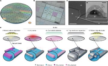

Superconducting-qubit lithography (Al/AlOx/Al junctions, Nb wiring, 300 mm)
300 mm junction lithography and post-fabrication frequency trimming (laser annealing, ABAA) set the frequency spread every superconducting architecture inherits.
Verdict. Real: 300 mm optical lithography yields 393/400 working qubits, at 5–7% frequency spread (10–14% in junction resistance); trimming lands 97.4% on target. Anderon is an LOI — demote if no non-IBM wafer ships by end-2027.
Λ = error-suppression factor per code-distance step; QBI = DARPA Quantum Benchmarking Initiative (Stage A concept → B R&D plan → C government V&V); G1–G7 = the report's goal classes (see Actors & economics).
Identity & lineage
A Josephson junction is two superconductors across a ~1–2 nm oxide barrier whose area and oxidation fix the critical current and hence the qubit frequency. This node is the process patterning those junctions and their niobium wiring at wafer scale — not a qubit. Lineage: e-beam Dolan-bridge Al/AlOx/Al junctions from the 2007 transmon (Koch et al., Yale), then 193 nm immersion lithography and etch on CMOS lines D[293].
Attributes. Carrier affinity 1.0 — fully fabricated: the manufacturing step itself, with no carrier, mobility, readout or control. Manufacturing — Nb wiring and Al/AlOx junctions on 200→300 mm silicon or sapphire; the error passed downstream is coherent (frequency offset, collision), not stochastic.
Physics & limits
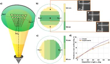
Ambegaokar–Baratoff ties critical current to normal-state resistance, and f01≈(√8EJEC-EC)/h, so Rn spread reaches frequency at half weight. imec measured ~8% RSD in junction resistance across a 300 mm wafer (7,872 test structures) and ~4% within a die, both for large junctions; at qubit junction sizes the area scatter adds, and qubit frequencies spread 5–7% RSD — 10–14% in resistance D[293]. That is a lattice problem, not a device problem: fixed-frequency neighbours must clear collision windows tens of MHz wide on a ~5 GHz qubit, so 5% spread (≈250 MHz, 1σ) leaves no collision-free yield at lattice scale. Trimming is a precondition, not an optimisation — alternating-bias assisted annealing moves junction resistance >70% and lands 97.4% of junctions on target D[294].
The second floor is dielectric loss: amorphous AlOx and interface oxides host two-level systems capping T1 in the tens-to-low-hundreds of µs. imec's 300 mm devices give median T1 75 µs, best 161 µs, best T2e 245 µs, over a 42–113 µs centre-to-edge gradient that is a process signature, not scatter D[293]. TLS drift hourly, and quasiparticle bursts set a floor lithography cannot touch Dfact. What moves it: epitaxial barriers and Ta/Nb base metal; tuneable couplers ease the first floor's frequency collisions, not the loss.
Engineering state of the art
Best on a genuine 300 mm CMOS line: 393 of 400 qubits functional D[293] — but at the frequency spread above, so trimming or tuneability is still required downstream.
table
| Year | Figure | Who | Tag+key |
|---|---|---|---|
| 2024-08 | ABAA trimming: 97.4% targeting success, >70% tuning range | Rigetti | D[294] |
| 2024-09 | 300 mm optical-litho transmons: 393/400 functional, median T1 75 µs, frequency RSD 5–7% | imec | D[293] |
| 2025-11 | Loon on 300 mm Albany: c-couplers, multilayer low-loss routing | IBM | C[49] |
| 2026-02 | Wafer-scale package: >500 qubits per 3-inch sapphire die, readout 97.5% median (n=54) | OQC | P[311] |
| 2026-05 | Anderon, pure-play 300 mm quantum foundry: $1 B CHIPS + $1 B IBM | IBM / US DoC | G[798] |
Dominant error term: coherent frequency error — spread, collisions, drift. TLS-limited T1 is what the process cannot remove.
Manufacturing, materials & supply chain
Dolan-bridge shadow evaporation still produces most published qubits; the CMOS route means 193i patterning, RIE, Nb wiring, TSVs, bump bonds. Its advantage is statistics and throughput, not coherence: imec's median T1 matches e-beam devices, its metrology does not. Trade press claims ~30× device output versus 200 mm; IBM's release states no multiple P[299]. Tooling is unremarkable, so the scarce asset is recipe and trimming capability; single points of failure are refrigerator capacity, high-resistivity silicon and sapphire, and Nb etch expertise shared with the SFQ chain. Cost per wafer is not quotable. Export exposure is indirect: the BIS rule of 2024-09-06 controls cryogenic wafer probers (3B904), sub-4.5 K cryogenic electronics (3A901) and quantum computers by qubit count and C-NOT error together, from 34 qubits at ≤ 10⁻⁴ to any error from 2,000 qubits (4A906) fact, but no ECCN names junction lithography G[301].
Control, readout & I/O burden
No control or readout of its own; it sets the ceiling others hit, through escape density and frequency targeting. OQC's package is the current bound: >500 qubits on one die, out-of-plane coax, no wire bonds, 56 nine-to-one readout multiplexing cells — and no per-qubit control lines as measured P[311], so it is a packaging result, not a processor. At 10³ per die the constraint is collisions; at 10⁴ escape density and routing, what Loon targets C[49]; at 10⁶ no fabricated design exists.
Role in the stack
Root node of the superconducting family: it requires nothing upstream and provides for transmon, fluxonium, the rf-SQUID flux qubit and planar bosonic modes, plus long-range c-couplers, millikelvin SFQ control, flux-DAC multiplexing, vertical signal delivery, multi-die packaging, multi-chip modules with l-couplers, and cryogenic microwave links. Architectures served: transmon, bosonic cat/GKP, dual-rail erasure, annealing. For a bosonic mode it is the planar alternative to machined 3D cavities. Fan-in is zero, yet its fan-out is the family's widest and every downstream node inherits its spread and yield. It adds nothing to the derived clock (derived clock = sum of the syndrome round: gate layers + transport + readout + reset, 0.65 µs on the transmon lattice) but bounds how many qubits reach it.
Evidence — how the numbers were measured
Frequency is predicted from junction resistance via Ambegaokar–Baratoff, then confirmed spectroscopically after packaging, so the statistic that matters is Rn RSD — published by nobody except imec D[293]. RB, XEB and cycle benchmarking measure a calibrated lattice, blind to dies discarded and pre-trim collision rates. ABAA's 97.4% is a targeting-success rate from an optimised study, not a worst-case bound D[294]. OQC's numbers are sub-sampled: readout over 54 of >500 sites, 105/108 operational on the characterised subset P[311]. Conflict: OQC's abstract gives a ~100 µs median for T1 and T2e together; its body gives T1 97 µs and T2e 129 µs over 105 qubits P[311].
IBM's 2026-05-21 release gives Anderon as a letter of intent subject to definitive documents, with no execution announced by 4 Sep 2026, yet IBM's 2026-08-26 HRL release already calls Anderon "its quantum wafer foundry". The "≈30× device output versus 200 mm" appears only in trade press [299]; IBM's own release states no multiple. The PatSnap H10N 60 counts [312] are portfolio-wide patent records. Not published: a per-wafer or per-qubit cost for any 300 mm superconducting-qubit line; a dated patent family specific to Nb/Al junction lithography at 300 mm; whether Google's Goleta purchase is fab capacity, and the wafer size of its Santa Barbara fabrication facility [805]; and whether the Nb wiring stack of imec's 300 mm line, which uses Al/AlOx/Al overlap junctions, matches IBM's approach.
Actors & economics
Who.
| Organisation | Role | Country | What exactly they do with this technology | Evidence |
|---|---|---|---|---|
| Anderon | supplier | US | Proposed pure-play 300 mm quantum wafer foundry | G[798] |
| IBM | developer | US | Fabricates Nighthawk and Loon on 300 mm Albany | C[49] |
| imec | research | BE | 300 mm optical-litho transmons, published yield | D[293] |
| Rigetti | developer | US | ABAA junction trimming on its own line | D[294] |
| OQC | developer | UK | Wafer-scale package, >500 qubits per die | P[311] |
| GlobalFoundries | supplier | US | $375 M CHIPS LOI, multi-modality foundry | G[300] |
| US Dept of Commerce | regulator | US | CHIPS letters of intent, $2.013 B | G[300] |
Money.
- 2026-05-21 · Anderon · CHIPS LOI plus IBM equity · $1 B CHIPS + $1 B IBM cash and IP · US Dept of Commerce · within $2.013 B across nine firms · LOI, unexecuted G[798]fact
- 2026-05-21 · GlobalFoundries · CHIPS LOI, multi-modality foundry · $375 M · US Dept of Commerce · — · LOI G[300]
- 2026-06-02 · IBM · commitment, quantum overall · >$10 B / 5 yr · — · announced C[57]
- 2026-08-26 · IBM · HRL acquisition completed, naming an Anderon collaboration · undisclosed · — · completed C[204]
Market & supply chain. No merchant superconducting-qubit foundry operates as of 4 Sep 2026: the 300 mm lines with published qubit data are IBM's captive Albany line and imec's research pilot, Google fabricates captively in Santa Barbara at an unpublished wafer size P[805], and the proposed merchant line is funded by its prospective customers' largest competitor. Binding scarcities are refrigerator capacity and process know-how, not tools; unit economics are not quotable. G3 and G4 pay directly, G7 indirectly; G1, G2, G5, G6 fund nothing.
IP & standards. PatSnap's landscape of 2026-06-30 counts 783 IBM and 357 Google patent records in superconducting devices (IPC H10N 60) P[312]fact. No patent family specific to 300 mm junction lithography carries a named assignee and year; no standards body governs these processes.
Roadmaps & track record. Anderon (promised 2026-05-21 · foundry serving vendors worldwide · status 2026-09-03: LOI only, yet IBM's 2026-08-26 release calls it "its quantum wafer foundry") G[798]C[204]. Rigetti/ABAA (2024-08 · production frequency targeting · in use under the 108-qubit product, whose 99.5% two-qubit target slipped to "later 2026") D[294]C[36]. IBM's fabrication milestones land on schedule; its merchant-access promise has no record.
Strategic reading. If 300 mm superconducting fab scales, IBM wins twice — vertically integrated, and landlord to everyone else's capacity. Fabless vendors win only with a neutral foundry, which does not exist. Losers are vendors whose differentiator is fabrication skill, not architecture. The threat is capture, not substitution: every superconducting architecture needs this node, and equipment suppliers have no bargaining power against its owner.
Outlook & open questions
Confirm by end-2027 if Anderon executes definitive CHIPS documents and fabricates for a named non-IBM customer; demote the merchant-foundry framing if only IBM designs emerge. Best case by 2029: two or more independent 300 mm lines with published cross-foundry uniformity and post-trim residuals below 1% frequency RSD. Worst case: Anderon stays captive. Open questions: does any line publish post-trim collision yield; can epitaxial barriers lift median T1 above 200 µs; does a merchant European or Asian line emerge?
References
- [36] Rigetti Computing, Inc., “Rigetti Announces General Availability of 108-Qubit System,” Apr. 7, 2026. [Online]. Available: https://investors.rigetti.com/
news-releases/ Cnews-release-details/ rigetti-announces-general-availability-108-qubit-system - [49] IBM, “IBM Delivers New Quantum Processors, Software, and Algorithm Breakthroughs on Path to Advantage and Fault Tolerance,” Nov. 12, 2025. [Online]. Available: https://newsroom.ibm.com/
2025-11-12-ibm-delivers-new-quantum-processors,-software,-and-algorithm-breakthroughs-on-path-to-advantage-and-fault-tolerance C - [57] IBM Quantum, “Why IBM is investing $10 billion into quantum computing,” Jun. 2, 2026. [Online]. Available: https://www.ibm.com/
quantum/ Cblog/ 10-billion-investment-faq - [204] IBM, “IBM Completes Acquisition of HRL Laboratories to Accelerate the Future of Quantum,” Aug. 26, 2026. [Online]. Available: https://newsroom.ibm.com/
2026-08-26-ibm-completes-acquisition-of-hrl-laboratories-to-accelerate-the-future-of-quantum C - [293] J. Van Damme et al., “Advanced CMOS manufacturing of superconducting qubits on 300 mm wafers,” Nature, vol. 634, no. 8032, pp. 74–79, Oct. 2024, doi: 10.1038/s41586-024-07941-9. D
- [294] D. P. Pappas et al., “Alternating-bias assisted annealing of amorphous oxide tunnel junctions,” Communications Materials, vol. 5, no. 1, Art. no. 150, Aug. 2024, doi: 10.1038/s43246-024-00596-z. D
- [299] L. James, “IBM spins off America's first quantum chip foundry with $2 billion in federal and private funding — newly-minted 'Anderon' foundry to offer 300mm quantum wafer fab and manufacturing services,” Tom's Hardware, May 26, 2026. [Online]. Available: https://www.tomshardware.com/
tech-industry/ Pquantum-computing/ ibm-spins-off-americas-first-quantum-chip-foundry-with-2-billion-in-federal-and-private-funding - [300] National Institute of Standards and Technology, “Department of Commerce Announces Letters of Intent With 9 Companies for $2 Billion to Accelerate U.S. Leadership in Quantum Computing,” NIST News, May 21, 2026. [Online]. Available: https://www.nist.gov/
news-events/ Gnews/ 2026/ 05/ department-commerce-announces-letters-intent-9-companies-2-billion - [301] US Department of Commerce, Bureau of Industry and Security, “Commerce Control List Additions and Revisions; Implementation of Controls on Advanced Technologies Consistent With Controls Implemented by International Partners,” Federal Register, vol. 89, p. 72926, Sep. 6, 2024. [Online]. Available: https://www.federalregister.gov/
documents/ G2024/ 09/ 06/ 2024-19633/ commerce-control-list-additions-and-revisions-implementation-of-controls-on-advanced-technologies - [311] O. W. Kennedy et al., “Design and Operation of Wafer-Scale Packages Containing >500 Superconducting Qubits,” arXiv:2602.12773, Feb. 2026. P
- [312] PatSnap, “Quantum Computing Patent Landscape 2026,” Jun. 30, 2026. [Online]. Available: https://www.patsnap.com/
resources/ Pblog/ rd-blog/ quantum-computing-patent-landscape/ - [798] IBM, “IBM and U.S. Department of Commerce Announce America's First Purpose-Built Quantum Foundry, Supported by Proposed $1 Billion CHIPS Award,” May 21, 2026. [Online]. Available: https://newsroom.ibm.com/
ibm-and-u-s-department-of-commerce-announce-americas-first-purpose-built-quantum-foundry G - [805] I. Hamm, “Google Buys 83,000-Square-Foot Campus in Goleta for $32.5M,” The Santa Barbara Independent, Aug. 24, 2026. [Online]. Available: https://www.independent.com/
2026/ P08/ 24/ google-buys-83000-square-foot-campus-in-goleta-for-32-5m/