Photonic IC foundry (SiN, BTO, TFLN, SNSPD on 300 mm) fab_pic
A CMOS foundry flow putting low-loss nitride waveguides, electro-optic switches, single-photon detectors and fibre attach on one 300 mm wafer.
Photonic IC foundry (SiN, BTO, TFLN, SNSPD on 300 mm)
GlobalFoundries Fab 8 for PsiQuantum (SiN 0.5 dB/m multimode but 1.8(2) dB/m single-mode, BTO switches, on-chip SNSPD at 93.4% median); TFLN/SiN for Xanadu; also ion integrated photonics and atom PIC traps.
Key references
Design space — attributes
- (a) carrier affinity
- photon (natural particle, engineered modes)
- (b) time · entangling
- —
- (c) readout
- —
- (d) mobility
- —
- (e) control
- —
- (f) error structure
- loss (erasure)
- (g) manufacturing
- photonic IC foundry
Evaluation space — dated attributes
The 0.5 dB/m figure is the multimode waveguide's; the single-mode Omega routing waveguide is 1.8(2) dB/m — two waveguides, not a conflict. The 98.9% median SNSPD efficiency sometimes quoted is superseded by 93.4%.
Standard records
Actors & goals — annotations
Edges
Used by 7 machines (4 primary · 3 alternate)
- photonics 6
- ETRI 8-photon silicon-photonic qubit chip ETRI (with KAIST and the University of Trento) paper ▨ ✅
- Omega chipset (Moreton Bay / Chicago systems unnamed) PsiQuantum paper product page press ▣ Fig. 1a–j (process modules, 300-mm wafer, cross-sections); §Technology stack ✅
- Carina QuiX Quantum ▨ ✅
- Aurora Xanadu paper press link ▤ Methods: Sources array; Refinery array; QPU array ✅
- Belenos Quandela product page press ▤ Methods: Architecture (12-mode Si3N4 photonic integrated circuit) ✅ (alternate)
- Lucy Quandela press ◌ 🔎 (alternate)
- defect spins 1
- Diamond-spin quantum computer prototype Fujitsu (with TU Delft and QuTech) press ▨ Overview of developed technologies: PIC fabrication for SnV centres (alumina optical waveguides) ✅ (alternate)
Pictures
Every picture carries the story of what it shows and its credit line.
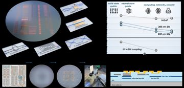
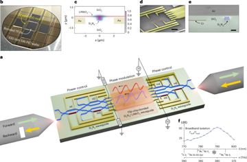
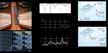
Photonic IC foundry (SiN, BTO, TFLN, SNSPD on 300 mm)
A CMOS foundry flow putting low-loss nitride waveguides, electro-optic switches, single-photon detectors and fibre attach on one 300 mm wafer.
Verdict. Demonstrated once, by one line (GlobalFoundries Fab 8 for PsiQuantum, 2025), with wafer-scale uniformity published but no die yield or ageing statistic; single-source risk defines the layer.
Λ = error-suppression factor per code-distance step; QBI = DARPA Quantum Benchmarking Initiative (Stage A concept → B R&D plan → C government V&V); G1–G7 = the report's goal classes (see Actors & economics).
Identity & lineage
The photonic IC foundry supplies the optics a photonic quantum computer is made of — SiN waveguides and delay lines, barium-titanate (BTO) or thin-film lithium niobate (TFLN) electro-optic switches, on-die superconducting nanowire single-photon detectors (SNSPDs), cryo-compatible fibre attach — on a 300 mm CMOS line with wafer-scale process control. A photonic qubit is never stored, only transmitted, so the figure of merit is a loss budget in decibels, not a coherence time. Lineage: ultra-low-loss dielectric waveguides (early 2010s, LioniX and UCSB), foundry access from about 2015 (AIM Photonics, imec), the first full quantum stack on 300 mm in 2025 D[169].
Attributes: carrier affinity natural-leaning (0.25), the line hosting no qubit but the modes that carry one; characteristic time not applicable, entangling downstream heralded, not deterministic; readout none intrinsically, but it supplies the on-chip SNSPDs, whose counting is destructive; mobility none — fixed lithography is what buys the photons theirs; control modality none, though it supplies the switches; error structure loss, seen by the code as heralded erasure; manufacturing a photonic-IC process line.
Physics & limits
Everything converts into one currency. Single-mode SiN routing at 1.8 ± 0.2 dB/m D[169] costs 34% of the photons per metre of on-chip delay; the wider multimode waveguide in the same process reaches 0.5 dB/m D[169]. Against an architectural budget near 0.5 dB for a whole fusion path, one BTO switch at 100 mdB spends a fifth of it, a fibre-to-chip transition at 52 ± 12 mdB a tenth, a median on-chip SNSPD at 93.4% efficiency 0.30 dB by itself D[169]. The dielectric floor is Rayleigh scattering from sidewall roughness, scaling with the mode's overlap with the etched interface, plus N–H absorption near 1520 nm that a 1150 °C anneal drives out. Both are beaten by weakening confinement: the 0.060 dB/m record used a 40 nm-thin core on a 100 mm wafer D[810], a geometry with millimetre bend radii. That is the trade — loss is bought with area, area with wafers — so a foundry routing waveguide is thirty times lossier than the record and must be. The other failure mode is phase: thermal gradients and stress birefringence detune interferometers, so a line that cannot hold film thickness ships chips needing per-die trimming. Moving the floor needs an electro-optic material whose Pockels coefficient shrinks switches faster than their loss grows — BTO's exceeds 1,000 pm/V against about 30 pm/V for lithium niobate D[169], which is why PsiQuantum and DARPA bet on it P[181].
Engineering state of the art
Best demonstrated is one wafer run; typical at scale is only partly defined, since Omega publishes spreads but no die yield D[169].
Records timeline
| Date | Figure | Who | Tag |
|---|---|---|---|
| 2018-09-24 | TFLN modulator: Vπ 1.4 V at 20 mm, insertion loss < 0.5 dB, 210 Gbit/s | Harvard (Lončar group) | D[811] |
| 2021-02-10 | SiN loss 0.060 dB/m, intrinsic Q 422 M (100 mm wafer, 40 nm core) | UCSB / Honeywell | D[810] |
| 2025-02-26 | 300 mm quantum PIC: SiN 1.8 ± 0.2 dB/m single-mode and 0.5 dB/m multimode, splitter 0.5 ± 0.2 mdB, BTO switch 100 mdB, median SNSPD 93.4%, fibre-to-chip 52 ± 12 mdB, fusion Bell 99.22 ± 0.12%, at ~2 K | PsiQuantum + GlobalFoundries | D[169] |
| 2026-06 | Edge coupling 0.085 dB per facet | Xanadu | C[172] |
The dominant budget term is not the waveguide but switch insertion loss, facet coupling and detector inefficiency — everything happening where the photon changes medium. The second is invisible: with no yield statistic, nobody can distinguish a process from a good die.
Manufacturing, materials & supply chain
The demonstrated flow is a 300 mm CMOS line with LPCVD (low-pressure chemical vapour deposition) nitride and a high-temperature anneal, BTO as an integrated active layer, SNSPDs patterned in situ, cryo-compatible fibre attach, at ~2 K rather than millikelvin D[169]. TFLN is made differently — ion-sliced bulk lithium niobate bonded to oxide — which is why HyperLight and Lightium are separate companies rather than modules in that line P[518]. The merchant market is otherwise 200 mm or smaller: LIGENTEC runs nitride on X-FAB's automotive-qualified 200 mm line and added X-FAB's SOI platform in 2026 C[812]; LioniX supplies TriPleX modules; imec and AIM Photonics run research lines.
Omega does publish spreads: on-chip SNSPD efficiency averages 88.9 ± 3.5% against its 93.4% median (screened detectors), BTO film thickness holds 3σ < 3% across the 300 mm wafer, and waveguide loss is 0.5 ± 0.3 dB/m multimode and 1.8 ± 0.2 dB/m single-mode D[169]. No die yield or 2 K thermal-cycle ageing data exists, and no foundry publishes quantum MPW or mask-set pricing, so cost per mode is unquotable as of 3 Sep 2026. Single points of failure: one 300 mm line has demonstrated the full stack; BTO deposition tooling is no merchant market; TFLN wafer supply is thin and concentrated; integrated SNSPDs exist at one vendor. Export-control exposure is indirect but real — the BIS interim final rule of 2024-09-06 created ECCNs 3A901 (cryogenic CMOS below 4.5 K), 3A904 (cryocoolers ≥ 600 µW below 0.1 K), 3B904 (cryogenic wafer probing), 3D901/3E901 and 4A906, with License Exception IEC G[301]. PIC processes and SNSPDs are not named; the cryogenic test equipment is.
A second, smaller line serves the near-visible band that atom and ion control needs: at 780 nm, silicon nitride (Si₃N₄) microresonators from a CMOS-compatible 150 mm multi-project-wafer process (deep-ultraviolet lithography, 1,200 °C anneal) reach a most-probable intrinsic quality factor Q₀ = 9.5 × 10⁶ over 721 measured resonances, a propagation loss of 6.3 dB/m P[886].
Control, readout & I/O burden
The I/O burden is fibre and bias lines. At 52 mdB per facet D[169] per-channel loss is affordable; the wall is assembly throughput, since 10⁶ modes need of order 10⁵–10⁶ alignment steps. Detection adds a bias line and an amplifier per SNSPD at 2 K, which by 10⁴ channels forces cryogenic readout ASICs — the cryo-CMOS controlled under 3A901 G[301] and now sold as a GlobalFoundries product line C[353]. Feed-forward must drive the switch within a delay line's lifetime, at MHz–GHz; the 100 mdB BTO switch at 2 K is both the enabling device and the item DARPA is paying to validate P[181]. At 10³ modes nothing binds; at 10⁴ fibre attach and channel count bind; at 10⁶ the constraints are wafer-scale integration, the cryoplant, and an unpublished yield.
Role in the stack
The layer floors two architectures as their primary process: fusion-based photonic computing (PsiQuantum, Quandela, QuiX) and continuous-variable/GKP computing (Xanadu); it is an alternate on five more — the boson sampler, colour-centre spin network nodes, trapped-ion QCCD, the linear Paul trap with laser addressing and the alkali Rydberg tweezer array. It provides single photons and squeezed modes, switches for routing and feed-forward, modulators, chip-to-fibre coupling, and the electro-optic chips transducers are built from. Its reach across families is a prospect, not yet a record: ion laser delivery and chip-generated atom tweezers are photonic-IC products too, and GlobalFoundries names trapped ions among the modalities its quantum unit serves C[353], but Quantinuum's ion waveguides come from Sandia's research complex (ct_ionlaser) and the atom chips on record use glass waveguides or Aeponyx's nitride with no foundry named (ct_pic_trap). If a 300 mm line takes those on, capital spent here stops being modality-specific — the least-correlated bet in the manufacturing layer. It replaces the bulk-optics table, and switching back costs area, alignment drift and any path past a few hundred modes. Derived clock = sum of the syndrome round: gate layers + transport + readout + reset — undefined on a fusion architecture, which runs none; this layer contributes only transport, roughly 5 ns per metre of on-chip delay, negligible against the 100 ns-class feed-forward the architecture needs D[169]. Neighbouring empty slots: a merchant 300 mm BTO switch process, a second source for integrated SNSPDs, any published wafer-level acceptance statistic.
Evidence — how the numbers were measured
Loss is measured two incompatible ways. Ring-resonator intrinsic Q gives the 0.060 dB/m record D[810] — one mode, one geometry, no routing. Spiral cut-back on a production reticle gives 1.8 dB/m D[169] — the waveguide the machine uses, and the only manufacturing number. Note that the main report's "0.5 dB/m" is the multimode figure from the Omega paper while the single-mode routing waveguide in the same paper is 1.8 ± 0.2 dB/m: both must be stated, they are not competing measurements D[169]. Fusion Bell fidelity, HOM visibility and detector efficiency are component metrics on selected dies, with no protocol converting them into a loss budget an architecture can be scored against, and no ageing data. No second group has reproduced any Omega figure on a second line; the only third-party check is DARPA's Stage C validation of the BTO switches, packaging and cryogenics, whose results are not public P[181]. The one conflict between sources is the PIXEurope budget: ≈€400 M per imec/ICFO G[582] against €380 M in trade press P[813]; trust the consortium release.
PIXEurope's budget is ≈€400 M in G[582] and €380 M in the consortium release P[813]. The dominance of a single Chinese ion-slicing supplier of TFLN wafers is widely cited but stated only qualitatively. Not published: dated 2025–2026 funding, capacity or loss figures for LioniX International; AIM Photonics' founding federal award and the wafer diameter of its Albany line; quantum MPW and mask-set prices at 300 mm, from any foundry, so no cost per mode can be quoted; and wafer-level yield or 2 K thermal-cycle ageing for BTO switches and integrated SNSPDs, from any actor — uniformity is public only as Omega's film-thickness, efficiency and loss spreads.
Actors & economics
Who.
| Organisation | Role | Country | What exactly they do | Evidence |
|---|---|---|---|---|
| GlobalFoundries | supplier (foundry) | US | Fab 8, Malta NY: the 300 mm line carrying Omega; Quantum Technology Solutions launched 2026-05-21 | C[353]D[169] |
| PsiQuantum | developer / customer | US, AU | Qualified the SiN + BTO + SNSPD + fibre-attach stack at 2 K | D[169] |
| imec | research foundry | BE | 300 mm CMOS and photonics, BTO-on-SOI heritage, PIXEurope partner | D[189]G[582] |
| LIGENTEC | supplier | CH, FR, BE | SiN on X-FAB's 200 mm line; added SOI 2026 | C[812] |
| LioniX International | supplier | NL | TriPleX SiN waveguides, module assembly | Cfact |
| HyperLight | supplier | US | TFLN modulators, Harvard spin-off | P[518] |
| AIM Photonics | research / foundry | US | DoD ManTech institute; PDK and Assembly Design Kit, 2026-05-25 | C[814] |
| Xanadu | developer | CA | TFLN/SiN CV chips; 0.085 dB/facet packaging; Toronto factory | C[172]C[178] |
| Quandela | developer | FR | GaAs quantum-dot sources; Lucy delivered to CEA/TGCC | C[176]fact |
| QuiX Quantum | developer | NL | SiN processors; Carina delivered to DLR, 2026-07 | C[177] |
Money.
- 2024-09 · HyperLight · Series B · $37 M · Summit Partners · closed P[518]
- 2024-09 · Lightium · seed · $7 M · Vsquared Ventures, Lakestar · closed P[518]
- 2024-11-24 · PIXEurope · EU pilot line · ≈€400 M · Chips JU, Spain, Catalonia · announced G[582]
- 2025-09-10 · PsiQuantum · Series E · $1 B at $7 B · BlackRock, Temasek, Baillie Gifford · closed fact
- 2026-03-26 · Xanadu · SPAC with Crane Harbor · ≈$302 M gross · Nasdaq/TSX XNDU · closed fact
- 2026-05-21 · GlobalFoundries · CHIPS letter of intent · $375 M · US Dept of Commerce · LOI, non-binding G[300]
- 2026-05-21 · PsiQuantum · CHIPS letter of intent · $100 M · US Dept of Commerce · LOI, non-binding G[300]
- 2026-07-22 · PsiQuantum · QBI Stage C expansion (BTO switches, packaging, cryogenics) · $125 M · DARPA · definitive fact
- 2026-08-28 · Xanadu · federal funding, Toronto factory · CAD 195 M · Government of Canada · announced C[178]
Market & supply chain. The enabling equipment is ordinary semiconductor capital (LPCVD/PECVD, immersion lithography, CMP, wafer bonding, MBE/PLD) from ASML, Lam, ASM, EVG and SUSS, in a market where quantum is a rounding error: good for cost, bad for influence. Concentration risk sits at the process, not the tool; unit economics are unquotable. G3 and G4 pay for this layer, G6 through fibre links and transducer chips, G7 through 2 K over millikelvin; G1 and G2 only via ion and atom optics, nothing in G5.
IP & standards. No dated patent count from a named database was retrieved for the PIC-foundry families; the one photonic family verified for this report is ORCA Computing's US 12,437,225 on linear-optical GHZ measurements, granted 2025-10-07 fact. There is no cross-foundry PDK standard — every design kit is proprietary and incompatible, the practical reason a customer cannot second-source. AIM Photonics publishes the most open kit C[814].
Roadmaps & track record. PsiQuantum, a commercially useful machine in Brisbane (promised 2024-04 · for end-2027 · groundbreaking slipped to 2026-06-17 and moved to Moreton Bay, cryoplant delivery due 2H 2027 Cfact, no 2026 hardware publication) Pfactfact; its DARPA tasking of 2026-07-22 frames the goal as a fault-tolerant machine "before 2033" P[181]. Xanadu loss 24.1× above threshold → 1.0× in 2030 (promised 2026-08-31 · nothing yet due) C[178]. PIXEurope pilot line (promised 2024-11 · for 2025 onward · no open-access run reported) G[582]. GlobalFoundries Quantum Technology Solutions (promised 2026-05-21 · LOI not yet definitive) C[353]G[300]. GlobalFoundries alone has a record of qualifying a process to production discipline; PsiQuantum has one paper and no second line; the European suppliers deliver at 200 mm, not at the loss-times-scale fault tolerance needs.
Strategic reading. If the layer succeeds the winner is the foundry, not the modality: GlobalFoundries collects a per-wafer annuity across five qubit technologies C[353] while PsiQuantum's differentiation narrows to architecture and cryogenics. If single-mode loss sticks near 1–2 dB/m both architectures stall and the value migrates to ion laser delivery, atom tweezers and networking — which is why it is worth funding either way. Substitution: bulk optics below a few hundred modes. Bargaining power sits with the foundry: switching lines means full requalification and a new PDK.
Outlook & open questions
Confirm if by end-2027 any actor publishes a wafer-level yield distribution for BTO switches or integrated SNSPDs at 300 mm; if a second line (imec, AIM Photonics, a PIXEurope member) publishes single-mode SiN loss ≤ 1.8 dB/m with monolithic detectors; or if Xanadu's loss factor falls below 10× threshold. Demote if PsiQuantum publishes no hardware result beyond Omega by mid-2027, or if the $375 M CHIPS LOI lapses. Best case by 2029: two qualified 300 mm lines, routing below 1 dB/m, switches under 50 mdB, published wafer maps. Worst case: one vendor, one paper, an LOI that never converts.
Open questions. (1) What is the die yield of an integrated SNSPD array on 300 mm, and why has nobody published it? (2) Is BTO manufacturable at volume, or a hero-die material DARPA is paying to find out about? (3) Who second-sources this layer if GlobalFoundries reprioritises?
References
- [169] K. Alexander et al., “A manufacturable platform for photonic quantum computing,” Nature, vol. 641, no. 8064, pp. 876–883, Feb. 2025, doi: 10.1038/s41586-025-08820-7. D
- [172] Xanadu, “Xanadu sets new industry benchmark in photonic chip packaging,” PR Newswire, Jun. 10, 2026. [Online]. Available: https://www.prnewswire.com/
news-releases/ Cxanadu-sets-new-industry-benchmark-in-photonic-chip-packaging-302796562.html - [176] Quandela, “Quandela delivers Lucy, the most advanced photonic quantum computer worldwide, to EuroHPC and GENCI at CEA's TGCC,” Oct. 23, 2025. [Online]. Available: https://www.quandela.com/
about-us/ Cnewsroom/ quandela-delivers-lucy-the-most-advanced-photonic-quantum-computer-worldwide-to-eurohpc-and-genci-at-ceas-tgcc/ - [177] QuiX Quantum, “QuiX Quantum Delivers Carina Core Hardware Platform to DLR QCI, Advancing Europe's Universal Photonic Quantum Computing Roadmap,” Jul. 14, 2026. [Online]. Available: https://www.quixquantum.com/
news/ Cquix-quantum-delivers-carina-core-hardware-platformto-dlr-qci - [178] Xanadu Quantum Technologies Limited, “Xanadu Charts Path to Over 1,000 Logical Qubits by 2031,” GlobeNewswire, Aug. 31, 2026. [Online]. Available: https://www.globenewswire.com/
news-release/ C2026/ 08/ 31/ 3353211/ 0/ en/ xanadu-charts-path-to-over-1-000-logical-qubits-by-2031.html - [181] M. Abdel-Kareem, “PsiQuantum Secures $125 Million Expanded Agreement with DARPA under QBI Program,” Quantum Computing Report, Jul. 22, 2026. [Online]. Available: https://quantumcomputingreport.com/
psiquantum-secures-125-million-expanded-agreement-with-darpa-under-qbi-program/ P - [189] P. Steinacker et al., “Industry-compatible silicon spin-qubit unit cells exceeding 99% fidelity,” Nature, vol. 646, no. 8083, pp. 81–87, Sep. 2025, doi: 10.1038/s41586-025-09531-9. D
- [300] National Institute of Standards and Technology, “Department of Commerce Announces Letters of Intent With 9 Companies for $2 Billion to Accelerate U.S. Leadership in Quantum Computing,” NIST News, May 21, 2026. [Online]. Available: https://www.nist.gov/
news-events/ Gnews/ 2026/ 05/ department-commerce-announces-letters-intent-9-companies-2-billion - [301] US Department of Commerce, Bureau of Industry and Security, “Commerce Control List Additions and Revisions; Implementation of Controls on Advanced Technologies Consistent With Controls Implemented by International Partners,” Federal Register, vol. 89, p. 72926, Sep. 6, 2024. [Online]. Available: https://www.federalregister.gov/
documents/ G2024/ 09/ 06/ 2024-19633/ commerce-control-list-additions-and-revisions-implementation-of-controls-on-advanced-technologies - [353] GlobalFoundries, “GlobalFoundries launches Quantum Technology Solutions to scale U.S. quantum manufacturing,” May 21, 2026. [Online]. Available: https://gf.com/
gf-press-release/ Also https://investors.gf.com/globalfoundries-launches-quantum-technology-solutions-to-scale-us-quantum-manufacturing/ news-releases/ . Cnews-release-details/ globalfoundries-launches-quantum-technology-solutions-scale-us - [518] optics.org, “Lithium niobate in vogue as thin-film developers raise cash,” Sep. 24, 2024. [Online]. Available: https://optics.org/
news/ Plithium-niobate-in-vogue-as-thin-film-developers-raise-cash - [582] imec, “The European Commission and Chips JU select the PIXEurope consortium to lead the European Pilot Line on Advanced Photonic Integrated Circuits,” Nov. 24, 2024. [Online]. Available: https://www.imec-int.com/
en/ Gpress/ european-commission-and-chips-ju-select-pixeurope-consortium-lead-european-pilot-line - [810] M. W. Puckett et al., “422 Million intrinsic quality factor planar integrated all-waveguide resonator with sub-MHz linewidth,” Nat. Commun., vol. 12, no. 1, Art. no. 934, Feb. 2021, doi: 10.1038/s41467-021-21205-4. D
- [811] C. Wang et al., “Integrated lithium niobate electro-optic modulators operating at CMOS-compatible voltages,” Nature, vol. 562, no. 7725, pp. 101–104, Oct. 2018, doi: 10.1038/s41586-018-0551-y. D
- [812] LIGENTEC, “About us_2026 - LIGENTEC.” [Online]. Available: https://www.ligentec.com/
about-our-story/ C - [813] PIC Magazine, “EU to establish €380 million pilot line for photonic integrated circuits,” Jan. 6, 2026. [Online]. Available: https://picmagazine.net/
article/ P123220/ EU_to_establish_%E2%82%AC380_million_pilot_line_for_photonic_integrated_circuits - [814] AIM Photonics, “News — AIM Photonics.” [Online]. Available: https://www.aimphotonics.com/
news C - [886] W. Sun et al., “A photonic integrated comb engine for ultracold quantum gases,” arXiv:2609.28294, Sep. 2026. P