300 mm CMOS foundry (spins, cryo-CMOS, superconducting wiring) fab_cmos
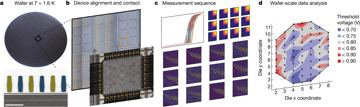
Industrial 300 mm CMOS lines fabricating quantum-dot spin qubits, cryo-CMOS controllers and superconducting wiring; the only qubit manufacturing route with wafer-scale yield statistics.
300 mm CMOS foundry (spins, cryo-CMOS, superconducting wiring)
Intel D1 EUV (24k devices/wafer, 96% tune-up), imec (2Q > 99%), GF 22FDX (1,024 dots), ST FD-SOI; GF now a multi-modality foundry ($375 M LOI).
Key references
Design space — attributes
- (a) carrier affinity
- fabricated
- (b) time · entangling
- —
- (c) readout
- —
- (d) mobility
- —
- (e) control
- —
- (f) error structure
- coherent / calibration
- (g) manufacturing
- CMOS foundry 300 mm
Evaluation space — dated attributes
Standard records
Actors & goals — annotations
Edges
Used by 20 machines (13 primary · 7 alternate)
- superconducting circuits 5
- IBM Quantum Blue Jay IBM blog ◌ 🔎 (alternate)
- IBM Quantum Heron r2 IBM paper paper press ▦ 🔎 (alternate)
- IBM Quantum Starling IBM blog ◌ 🔎 (alternate)
- KRISS domestic superconducting QPU Korea Research Institute of Standards and Science press press ▨ 🔎 (alternate)
- Qolab devices at the IQCC Qolab ▦ §Window-junction process (semiconductor-compatible; scales to 300 mm wafers) ✅ (alternate)
- trapped ions 6
- IonQ Superion 10K IonQ press ▨ SkyWater paragraph; Superion 10K paragraph ✅
- Superion 256 IonQ press press ▨ ✅
- Apollo Quantinuum blog ▥ §What is Apollo? (trap chip fabricated using standard CMOS processing) ✅
- NFQC-1k QUDORA Technologies-led consortium (TU Braunschweig, Leibniz University Hannover, PTB, Forschungszentrum Jülich, NXP Semiconductors Germany, AQT Germany) press ▨ pilot-line paragraph; partner list (NXP) ✅
- Sol Quantinuum blog ▥ §What is Apollo? (Apollo trap chip: 2D array fabricated using standard CMOS processing, CMOS electronics) ✅ (alternate)
- iQPU / UQConnect Universal Quantum press ▨ 🔎 (alternate)
- semiconductor spins 9
- Diraq 8-qubit silicon spin quantum computer at Equinix Sydney Diraq (with Equinix) ▨ manufacturing paragraph (existing semiconductor foundries) ✅
- foundry 8-qubit array Diraq paper press ▤ §IV.1 Methods: Fabrication ✅
- RacQ (Bell-1) Equal1 product page blog blog ▦ UnityQ page ('Built on GlobalFoundries 22FDX') ✅
- Groove Quantum 18-qubit germanium spin processor Groove Quantum press ◌ 🔎
- Hitachi x Intel 18A spin programme Hitachi + Intel K.K. + AIST (G-QuAT) press press ▨ 🔎
- HRL exchange-only silicon spin processor (18 EO qubits from 54 quantum dots) HRL Laboratories (IBM since 26 Aug 2026) paper press ▤ Main text: cryo-controller; Methods: Qubit chip ✅
- Tunnel Falls Intel paper press press ▤ Abstract (300 mm manufacturing line; EUV lithography) ✅
- QM-One Quantum Motion ▤ §VI.A Fabrication details ✅
- Alloy Pioneer (Quobly) Quobly press ▨ 🔎
Pictures
Every picture carries the story of what it shows and its credit line.


300 mm CMOS foundry (spins, cryo-CMOS, superconducting wiring)
Industrial 300 mm CMOS lines fabricating quantum-dot spin qubits, cryo-CMOS controllers and superconducting wiring; the only qubit manufacturing route with wafer-scale yield statistics.
Verdict. Uniformity is proven (96% device yield, sub-nm CD); fidelity is not yet a foundry deliverable. Demote if no 300 mm device with >20 qubits and all-pairs 2Q ≥ 99.5% appears by end-2027.
Λ = error-suppression factor per code-distance step; QBI = DARPA Quantum Benchmarking Initiative (Stage A concept → B R&D plan → C government V&V); G1–G7 = the report's goal classes (see Actors & economics).
Identity & lineage
This node is a manufacturing regime, not a qubit: 300 mm CMOS production lines making gate-defined quantum-dot arrays (Si/SiGe, SiMOS, Ge), their cryo-CMOS ASICs, and superconducting qubit and wiring layers. A quantum dot is an accumulation-mode transistor at single-electron occupancy; at 45–100 nm pitch the foundry supplies uniformity, interface quality and isotopic control, not resolution, across tens of thousands of devices per wafer with cryogenic wafer-level test.
CEA-Leti opened the route in 2016 with a spin qubit in a 28 nm FD-SOI flow D[793]. Intel and QuTech made the first all-optically patterned 300 mm qubits in March 2022 D[794], fixing since 2022; Intel added EUV arrays and 1.6 K wafer statistics in 2024 D[199], [766]. imec produced 300 mm transmons in 2024 D[293] and, with Diraq, unit cells above 99% in 2025 D[189]. GlobalFoundries' 22FDX became the merchant option in 2025 D[767], ST started ²⁸Si FD-SOI lots in December 2025 P[795], and US CHIPS letters of intent followed in May 2026 G[300].
Attributes (technology graph):
a, carrier affinity: fabricated, 1.0; the node is fabrication itself.
b, characteristic time: none; no gate time or entangling mode.
c, readout: none.
d, mobility and connectivity: none.
e, control modality: none.
f, error structure: coherent; device-to-device variability read as calibration error.
g, manufacturing: CMOS.
Physics & limits
Mechanism. The fab fixes four inherited quantities: geometric uniformity, critical dimension within 0.5 nm at 45–100 nm pitch D[199]; electrostatic disorder, a random threshold-voltage spread of 59 mV on Intel Si/SiGe D[766]; isotopic purity, 800 ppm residual ²⁹Si at Intel D[199] and 400 ppm at imec D[189]; and interface quality, which sets charge noise and, in Si/SiGe, the valley-splitting distribution.
Scales. T2*/T2echo reach 5/205 µs on ²⁸Si Si/SiGe against 0.6/98 µs on natural silicon D[766]; Hahn-echo T2 reaches 1.31 ms on imec SiMOS D[197].
Floor. For spins it is material: residual ²⁹Si, interface charge noise and the Si/SiGe valley-splitting tail that turns some dots into leakage sinks. For transmons it is junction targeting: across a 300 mm wafer qubit frequencies spread 5–7%, i.e. 10–14% in junction resistance at qubit junction sizes (the ~8% resistance spread is that of large junctions) D[293], an order above collision-free lattice needs; alternating-bias annealing (97.4% targeting D[294]) is post-fabrication, not a foundry property.
As the code sees it: coherent, calibratable error (HRL attributes about 80% of CNOT error on its 54-dot array to control and calibration D[190]) plus leakage and slow drift; nothing is erasure-convertible; wafer gradients D[293] become spatially correlated error. Moving the floor needs 10-ppm-class ²⁸Si, engineered valley splitting (simulation only S[796]), Ge/SiGe holes or in-flow junction trimming.
Engineering state of the art
Best demonstrated: four Diraq/imec unit cells, every operation above 99% (1Q 99.97%, CZ 99.04–99.56%, SPAM 99.95% at 100 µs), gate-set tomography, September 2025 D[189]fact. Typical at scale: Intel's 232 twelve-dot devices on one wafer gave 99.8% dot and 96% full-device yield, May 2024 D[766]; unmodified 22FDX gave 28–40% "good dot" yield over 1,024 dots, January 2025 D[767]; imec's eight-qubit array validated one pair of four, July 2026 D[197].
table
| year | figure | who | tag+key |
|---|---|---|---|
| 2016 | spin qubit in a 300 mm 28 nm FD-SOI flow | CEA-Leti | D[793] |
| 2022-03 | >10,000 dot arrays per wafer; 1Q 99.0–99.1% | Intel/QuTech | D[794] |
| 2024-09 | 300 mm transmons: median T1 75 µs, 98.25% yield | imec/KU Leuven | D[293] |
| 2024-12 | >24,000 devices per wafer, CD < 0.5 nm (EUV) | Intel | D[199] |
| 2025-01 | 1,024 dots on 22FDX, 1:1,024 cryo-CMOS mux, < 10 min | Quantum Motion/GF | D[767] |
| 2025-09 | CZ 99.04–99.56% on 300 mm SiMOS, 4 of 4 devices > 99% | Diraq/imec | D[189] |
| 2026-04 | 4 K CMOS controller (366 DACs, ≤ 3.5 W) runs d=5 repetition code, Λ = 4.7 | HRL | D[190]fact |
Dominant error term: the 2Q plateau at 99.0–99.6% is charge noise plus exchange calibration D[189], [190]; 100 µs readout for 99.9%-class SPAM D[189] sets a 100–300 µs cycle; no 300 mm device above twelve qubits has published all-pairs 2Q; for transmons the limit is junction spread, not coherence D[293].
Manufacturing, materials & supply chain
Platforms. Intel D1: Si/SiGe wells, immersion and EUV lithography, cryo-prober screening D[199], [766]. imec: SiMOS with overlapping polysilicon gates below 100 nm pitch on 400 ppm ²⁸Si D[189], plus a transmon flow with dry-etched overlap junctions D[293]. FD-SOI: GlobalFoundries 22FDX (Quantum Motion D[767]; Equal1 C[797]) and ST 28 nm at Crolles on Soitec ²⁸Si substrates, first lots December 2025 P[795]. HRL and SkyWater run 200 mm D[190]C[19].
Yield. 96% device yield on a quantum-optimised flow D[766] against 28–40% on a merchant flow D[767] is this node's central number.
Cost and energy. No foundry publishes a quantum wafer price; Diraq's < $1 per qubit target R[211] and vendors' rack-scale claims C[200], [355], [771] are unaudited.
Supply chain. Lines: Intel (captive); imec, coordinator of the EU SPINS pilot line G[770]; GlobalFoundries' Quantum Technology Solutions unit C[353]; IBM Albany, becoming Anderon for superconducting wiring, TSVs and bumps C[798]; SkyWater, 200 mm, IonQ-owned since 2026-07-31 C[19]. Materials: enriched ²⁸Si, historically Russian, now also from ASP Isotopes in Pretoria (commercial since 2025-03-27) C[347] and from ORNL and PNNL as 99.9999% ²⁸Si silane (US DOE, announced 2026-07-16) G[348]; Silex completed a plant for up to 20 kg per year in June 2026, commissioning late 2026, for SQC C[799]. Equipment: cryogenic wafer probers from Bluefors/Afore (< 2 K, 300 mm, 768 DC, 48 RF lines) C[800] and FormFactor C[801]. Single points of failure: EUV dots only at Intel and imec; a prober duopoly; ²⁸Si from a handful of enrichers.
Export control. BIS's rule of 2024-09-06 controls cryogenic CMOS ICs for ≤ 4.5 K (ECCN 3A901), cryogenic systems ≥ 600 µW at ≤ 0.1 K (3A904), cryogenic wafer probers (3B904) and quantum computers by qubit count and C-NOT error together, from 34 qubits at ≤ 10⁻⁴ to any error from 2,000 qubits (4A906) fact, with License Exception IEC for allies G[301]fact; EU and UK lists match. The same rule controls silicon and germanium enriched beyond set isotope fractions — epitaxial layers, hydrides such as silane, bulk and oxides (3C907–3C909) G[301].
Control, readout & I/O burden
Multiplexing moves on-die or in-package: a 1:1,024 cryo-CMOS multiplexer on 13 lines D[767]; imec's multiplexer routing transmon pulses below 15 mK with > 99.9% 1Q preserved D[802]; a 32-cell 28 nm FD-SOI chip at 7 mK, ~20 nW/MHz per cell D[551]; HRL's 4 K controller, 366 DACs at ≤ 3.5 W (~10 mW per channel), running a repetition code D[190]; IBM's 4 K controller at 23 mW per qubit D[296]. Crossbar sharing needs T = 6√g − 1 lines for a square array of g dots (23 for 16) D[520].
Walls. 10³: per-qubit lines suffice; the burden is tune-up time. 10⁴: at IBM's 23 mW per qubit D[296] the 4 K load is 230 W, at HRL's 3.5 W per 18 qubits D[190] about 2 kW — over a hundred times the 2 W 4 K stage of a Bluefors XLD1000sl, and above the 200 W of Fermilab's Colossus, the largest plant in the resource review S[550] — forcing ≥ 10:1 multiplexing or millikelvin nW-class cells. 10⁶: only crossbar sharing (~6,000 lines D[520]) plus millikelvin CMOS or SFQ closes; whether shared control keeps coherent error below threshold is open. Latency: spin cycles are readout-bound, 100 µs integration D[189].
Role in the stack
A layer-10 root: it requires nothing and provides the dot arrays and cryo-ASICs the quantum-dot spin architecture assumes, its primary home; it is an alternate on the transmon lattice with tunable couplers, trapped-ion QCCD and trapped ions with electronic gates. It replaces STM-lithography donor fabrication (11-qubit registers, serial, no foundry route D[192]); for ion traps it is the alternative to MEMS trap fabs, the switching price being CMOS re-qualification, paid by Oxford Ionics (part of IonQ since 2025-09-17), whose 99.99% two-qubit fidelity on standard-fab chips is reported in an IonQ release C[446]fact. Here natural carriers (trapped ions) inherit semiconductor manufacturing. Derived clock = sum of the syndrome round: gate layers + transport + readout + reset for the architecture; this node adds no term; the quantum-dot spin architecture's derived round is 8.5 µs, readout-set, against a measured 100–300 µs cycle D[189]. Conveyor shuttling over an effective 10 µm (back and forth) at 99.5% D[196], shown on a Delft-made device, is what uniform 300 mm gates must reproduce. Neighbouring empty slots: no spin-module interconnect (300 mm photonics is the candidate, unproven at millikelvin) and no fabricated cryogenic decoder; a cryo-CMOS predecoder design claims 3,780× syndrome-bandwidth reduction below 0.56 mW S[733].
Evidence — how the numbers were measured
Yield numbers come from cryo-probers at 1.6–1.7 K (automated tune-up, turn-on/pinch-off and charge-sensing criteria D[199], [766]): transistor statistics. Fidelities come from few devices in dilution refrigerators: gate-set tomography (12,263 sequences) for the unit cells D[189], randomised benchmarking on Tunnel Falls D[199], T1/T2 wafer maps for transmons D[293].
Not captured: (1) 1.6 K probing cannot see valley splitting, exchange or coherence, so device yield says nothing about qubit yield; (2) selection: 4 of 20 imec devices characterised D[189], 6 of > 10,000 arrays cooled in 2022 D[794]; (3) criteria: 28–40% and 96% define "working" differently D[766], [767]; (4) no simultaneous all-pairs 2Q on any 300 mm array D[197]; (5) ageing: 3.7% junction drift in 146 days D[293] is absent from fidelity claims.
Replication: imec's SiMOS numbers reproduce across four devices and two institutions D[189]; Intel's are single-vendor. Flagged: Quantum Motion's "first full-stack silicon CMOS quantum computer" without published fidelities C[200]; Equal1's commercial-process dots without qubit metrics C[797].
SPAM for the imec/Diraq unit cells is 99.95% at 100 µs [189], against 99.9% recorded for imec's 300 mm line (2025). Intel's yield figures all come from [766], on 232 twelve-dot devices of one wafer — 99.8% of dots, 96% of full devices, 91% charge-sensing success; [199] restates the 96%, citing [766]. Not published: the dates of Silex's A$5.1 M Defence Trailblazer and A$4.35 M SQC funding [799].
Actors & economics
Who.
| Organisation | Role | Country | What they do | Evidence |
|---|---|---|---|---|
| Intel | developer; captive supplier | US | Si/SiGe EUV arrays; cryo-prober wafer statistics; 12-qubit chip at Argonne | D[199], [766]; G[207] |
| imec | research; supplier | BE | 300 mm SiMOS dots, transmons, millikelvin multiplexer; SPINS coordinator | D[189], [293], [802]; G[770] |
| GlobalFoundries | supplier (merchant foundry) | US | 22FDX dots and cryo-CMOS; Quantum Technology Solutions unit; $375 M LOI | C[353], [803]; G[300] |
| IBM | developer; supplier | US | Anderon: 300 mm superconducting wafers, TSVs, bumps; $1 B LOI | C[10], [798]; G[300] |
| Diraq | developer | AU | SiMOS unit cells at imec; QBI Stage B; CHIPS LOI up to $38 M | D[189], [197]; G[65], [300] |
| Quantum Motion | developer | UK | 22FDX 1,024-dot arrays; NQCC system; QBI Stage B | D[767]; C[200]; G[65] |
Money.
| date | actor | event | amount | lead or programme | cumulative | status |
|---|---|---|---|---|---|---|
| 2025-11-06 | Diraq; Quantum Motion; SQC | grant | up to $15 M each | DARPA QBI Stage B | — | definitive G[65]fact |
| 2026-01-15 | Equal1 | round | $60 M | ISIF | > $85 M | closed C[771]fact |
| 2026-04-03 | imec + 25 partners | grant | €50 M | EU Chips JU SPINS pilot line | — | announced G[770] |
| 2026-05-07 | Quantum Motion | Series C | $160 M | DCVC, Kembara | — | closed C[355]fact |
| 2026-05-21 | GlobalFoundries | CHIPS LOI | $375 M | US Commerce ($2.013 B over nine LOIs) | — | LOI, non-binding G[300]C[353]fact |
| 2026-05-21 | IBM (Anderon) | CHIPS LOI | $1 B + $1 B IBM cash | US Commerce | — | LOI, non-binding G[300]C[798] |
| 2026-05-21 | Diraq | CHIPS LOI | up to $38 M | US Commerce | > $100 M raised Pfact | LOI, not awarded G[300] |
| 2026-06-03 | Quobly | Series A | €115 M | Bpifrance, SEALSQ, STMicroelectronics | €134 M | closed P[804]fact |
| 2026-06 | Silex Systems | Q-Si plant completed | A$5.1 M + A$4.35 M | Defence Trailblazer; SQC | — | commissioning late 2026 C[799] |
| 2026-07-23 | IBM | M&A: HRL Laboratories | undisclosed | — | — | announced; closed 2026-08-26; potential plans for spin qubits at Anderon C[10]factfact |
| 2026-07-31 | IonQ | M&A: SkyWater | $15.00 + 0.4883 IonQ shares per share (~$1.8 B) | — | — | closed C[19]fact |
Market & supply chain. Quantum is immaterial to foundry revenue. Concentration: two EUV-capable dot lines, one merchant FD-SOI option (ST entering), a prober duopoly, a handful of ²⁸Si enrichers. Unit economics: unpublished beyond Diraq's target R[211]. Payers: G4 for 10⁶-qubit CMOS density; G7, as of 3 Sep 2026, for rack-scale spin systems; superconducting vendors buy Anderon/GF wiring for G2–G4; ion vendors buy standard-fab traps for G2, G3, G7.
IP & standards. Portfolios: Intel, HRL, Diraq/UNSW, Quantum Motion/UCL, Quobly (CEA/CNRS licences), Equal1; no litigation public; no dated family count from a named database found. SPINS promises quantum PDKs and multi-project-wafer access G[770]; GF markets FDX cryogenic models C[353]; no open cryogenic device-model standard exists.
Roadmaps & track record. Intel (promised 2022 · wafer-scale qubits · delivered 2024, Argonne 2026-01-06 G[207]fact; no successor or roadmap as of 2026-09-03). Diraq (promised 2026-07-09 · "thousands" by 2029, restated 2026-08-27 as 150,000 physical · eight qubits shown D[197]R[211]fact). Quantum Motion (promised 2025-01 · NQCC system · delivered 2025-09-15, no published fidelity C[200], [803]). Quobly (promised 2025-12 · ST-lot metrics Q1 2026 P[795] · none found as of 2026-09-03). GF, Anderon: no wafer dates promised C[353], [798]. Credibility: imec/Diraq (peer-reviewed, replicated) first; Intel manufactures without a product path; Quantum Motion and Equal1 deliver systems without peer-reviewed metrics (Equal1's RacQ, sold as Bell-1 until May 2026, is installed at ESA's Frascati centre, announced by ESA on 2026-07-15 fact and by Equal1 on 2026-07-31 Cfact), Quobly none yet; roadmap slides last.
Strategic reading. Success rewards foundries and suppliers (GF, imec, ST/Soitec, Bluefors) and spin vendors whose bill of materials shrinks to wafers plus racks; bespoke routes (STM lithography, university lift-off) and MEMS trap fabs lose. Supplier bargaining power is high (few lines, quantum revenue immaterial), but three or four substitutable lines and state money cap what foundries extract. Substitution threats: Ge/SiGe holes, photonic-interconnect fabs, SFQ against cryo-CMOS.
Outlook & open questions
Milestones, 12–24 months: (1) a 300 mm device with > 20 qubits and published all-pairs 2Q ≥ 99.5% confirms; none by end-2027 demotes; (2) SPINS multi-project-wafer runs with a public quantum PDK; (3) GF's LOI made definitive, a named 22FDX quantum product; (4) a spin-qubit lot at Anderon from HRL, IBM-owned since 2026-08-26; (5) Intel naming a Tunnel Falls successor or exiting.
2029 best case: two merchant 300 mm lines with quantum PDKs, 10³-dot arrays with on-die multiplexing, 2Q ≥ 99.5% typical, a below-threshold spin memory. Worst: merchant yields at tens of percent, 2Q at 99–99.6%, roadmaps cut again, GF's unit reduced to packaging for superconducting and photonic customers.
Open questions: can valley splitting and charge noise be made wafer-uniform, or must every array be post-selected? What is the qubit-fidelity yield of a 300 mm flow? Does shared control keep coherent error below threshold? Can in-flow junction targeting reach sub-percent? Watch the first fidelity-yield number, SPINS' first multi-project wafer, definitive CHIPS awards, Intel.
References
- [10] IBM, “IBM to Acquire HRL Laboratories to Power the Future of Quantum,” Jul. 23, 2026. [Online]. Available: https://newsroom.ibm.com/
2026-07-23-ibm-to-acquire-hrl-laboratories-to-power-the-future-of-quantum C - [19] IonQ, “IonQ Completes Acquisition of SkyWater Technology,” Jul. 31, 2026. [Online]. Available: https://www.ionq.com/
news/ Cionq-completes-acquisition-of-skywater-technology - [65] DARPA, “Stage B selection,” Nov. 6, 2025. [Online]. Available: https://www.darpa.mil/
research/ Gprograms/ quantum-benchmarking-initiative/ stage-b-selection - [189] P. Steinacker et al., “Industry-compatible silicon spin-qubit unit cells exceeding 99% fidelity,” Nature, vol. 646, no. 8083, pp. 81–87, Sep. 2025, doi: 10.1038/s41586-025-09531-9. D
- [190] Members of the HRL Quantum Team and Collaborators, “A digitally controlled silicon quantum processing unit,” arXiv:2604.16216, Apr. 2026. D
- [192] H. Edlbauer et al., “An 11-qubit atom processor in silicon,” Nature, vol. 648, no. 8094, pp. 569–575, Dec. 2025, doi: 10.1038/s41586-025-09827-w. arXiv:2506.03567. D
- [196] M. De Smet et al., “High-fidelity single-spin shuttling in silicon,” Nat. Nanotechnol., vol. 20, no. 7, pp. 866–872, Jun. 2025, doi: 10.1038/s41565-025-01920-5. D
- [197] A. Nickl et al., “Eight-qubit operation of a 300 mm SiMOS foundry-fabricated device,” Nat. Commun., vol. 17, no. 1, Art. no. 5878, Jul. 2026, doi: 10.1038/s41467-026-74597-6. D
- [199] H. C. George et al., “12-spin-qubit arrays fabricated on a 300 mm semiconductor manufacturing line,” Nano Lett., vol. 25, no. 2, pp. 793–799, Dec. 2024, doi: 10.1021/acs.nanolett.4c05205. arXiv:2410.16583. D
- [200] Quantum Motion, “Quantum Motion Delivers the Industry's First Full-Stack Silicon CMOS Quantum Computer,” Sep. 15, 2025. [Online]. Available: https://quantummotion.com/
quantum-motion-delivers-the-industrys-first-full-stack-silicon-cmos-quantum-computer/ C - [207] L. Hesla, “Argonne launches silicon quantum processor collaboration with Intel,” Argonne National Laboratory, Jan. 6, 2026. [Online]. Available: https://www.anl.gov/
article/ Gargonne-launches-silicon-quantum-processor-collaboration-with-intel - [211] F. Elliott, “Diraq charts course to utility-scale quantum computing with millions of spin qubits on a single silicon chip,” Diraq, Aug. 27, 2026. [Online]. Available: https://www.diraq.com/
newsdesk/ Rdiraq-sets-roadmap-for-utility-scale-quantum-computing-with-millions-of-qubits-on-a-single-silicon-chip - [293] J. Van Damme et al., “Advanced CMOS manufacturing of superconducting qubits on 300 mm wafers,” Nature, vol. 634, no. 8032, pp. 74–79, Oct. 2024, doi: 10.1038/s41586-024-07941-9. D
- [294] D. P. Pappas et al., “Alternating-bias assisted annealing of amorphous oxide tunnel junctions,” Communications Materials, vol. 5, no. 1, Art. no. 150, Aug. 2024, doi: 10.1038/s43246-024-00596-z. D
- [296] D. Underwood et al., “Using Cryogenic CMOS Control Electronics to Enable a Two-Qubit Cross-Resonance Gate,” PRX Quantum, vol. 5, no. 1, Art. no. 010326, Feb. 2024, doi: 10.1103/PRXQuantum.5.010326. D
- [300] National Institute of Standards and Technology, “Department of Commerce Announces Letters of Intent With 9 Companies for $2 Billion to Accelerate U.S. Leadership in Quantum Computing,” NIST News, May 21, 2026. [Online]. Available: https://www.nist.gov/
news-events/ Gnews/ 2026/ 05/ department-commerce-announces-letters-intent-9-companies-2-billion - [301] US Department of Commerce, Bureau of Industry and Security, “Commerce Control List Additions and Revisions; Implementation of Controls on Advanced Technologies Consistent With Controls Implemented by International Partners,” Federal Register, vol. 89, p. 72926, Sep. 6, 2024. [Online]. Available: https://www.federalregister.gov/
documents/ G2024/ 09/ 06/ 2024-19633/ commerce-control-list-additions-and-revisions-implementation-of-controls-on-advanced-technologies - [347] ASP Isotopes Inc., “ASP Isotopes Inc. Commences Commercial Production of Enriched Silicon-28 at its Second Aerodynamic Separation Process (ASP) Enrichment Facility,” Mar. 27, 2025. [Online]. Available: https://ir.aspisotopes.com/
news-events/ Cpress-releases/ detail/ 56/ asp-isotopes-inc-commences-commercial-production-of - [348] U.S. Department of Energy, “DOE Advances Domestic Supply of Silicon, Germanium Isotopes for Quantum Computing,” HPCwire, Jul. 16, 2026. [Online]. Available: https://www.hpcwire.com/
off-the-wire/ Gdoe-advances-domestic-supply-of-silicon-germanium-isotopes-for-quantum-computing/ - [353] GlobalFoundries, “GlobalFoundries launches Quantum Technology Solutions to scale U.S. quantum manufacturing,” May 21, 2026. [Online]. Available: https://gf.com/
gf-press-release/ Also https://investors.gf.com/globalfoundries-launches-quantum-technology-solutions-to-scale-us-quantum-manufacturing/ news-releases/ . Cnews-release-details/ globalfoundries-launches-quantum-technology-solutions-scale-us - [355] Quantum Motion, “Quantum Motion Raises $160 Million Series C to Deliver Quantum Computing's "Transistor Moment,” May 7, 2026. [Online]. Available: https://quantummotion.com/
quantum-motion-raises-160-million-series-c-to-deliver-quantum-computings-transistor-moment/ C - [446] IonQ, “IonQ Achieves Landmark Result, Setting New World Record in Quantum Computing Performance,” Oct. 21, 2025. [Online]. Available: https://www.ionq.com/
news/ Cionq-achieves-landmark-result-setting-new-world-record-in-quantum-computing - [520] F. Borsoi et al., “Shared control of a 16 semiconductor quantum dot crossbar array,” Nat. Nanotechnol., vol. 19, no. 1, pp. 21–27, Jan. 2024, doi: 10.1038/s41565-023-01491-3. D
- [550] S. Kawabata, “Integration and Resource Estimation of Cryoelectronics for Superconducting Fault-Tolerant Quantum Computers,” arXiv:2601.03922, Jan. 2026. S
- [551] S. K. Bartee et al., “Spin-qubit control with a milli-kelvin CMOS chip,” Nature, vol. 643, no. 8071, pp. 382–387, Jul. 2025, doi: 10.1038/s41586-025-09157-x. D
- [733] A. Knapen et al., “Pinball: A Cryogenic Predecoder for Surface Code Decoding Under Circuit-Level Noise,” arXiv:2512.09807, Dec. 2025. S
- [766] S. F. Neyens et al., “Probing single electrons across 300-mm spin qubit wafers,” Nature, vol. 629, no. 8010, pp. 80–85, May 2024, doi: 10.1038/s41586-024-07275-6. D
- [767] E. J. Thomas et al., “Rapid cryogenic characterization of 1,024 integrated silicon quantum dot devices,” Nat. Electron., vol. 8, no. 1, pp. 75–83, Jan. 2025, doi: 10.1038/s41928-024-01304-y. D
- [770] imec, “Quantum pilot line 'SPINS' launched with EU support,” Apr. 3, 2026. [Online]. Available: https://www.imec-int.com/
en/ Gpress/ semiconductor-based-quantum-pilot-line-spins-launched-eu-support - [771] University College Dublin, “Equal1 Announces $60 million in Funding to Accelerate Quantum Computing using Existing Semiconductor Manufacturing,” UCD Innovation, Jan. 15, 2026. [Online]. Available: https://www.ucd.ie/
innovation/ Cnews-and-events/ 2026/ equal1-announces-funding-round/ - [793] R. Maurand et al., “A CMOS silicon spin qubit,” Nat. Commun., vol. 7, Art. no. 13575, Nov. 2016, doi: 10.1038/ncomms13575. D
- [794] A.-M. Zwerver et al., “Qubits made by advanced semiconductor manufacturing,” Nat. Electron., vol. 5, no. 3, pp. 184–190, Mar. 2022, doi: 10.1038/s41928-022-00727-9. D
- [795] C. Knowles, “Quobly runs silicon-28 quantum wafers through ST fab,” IT Brief Asia, Dec. 12, 2025. [Online]. Available: https://itbrief.asia/
story/ Pquobly-runs-silicon-28-quantum-wafers-through-st-fab - [796] M. P. Losert et al., “Practical strategies for enhancing the valley splitting in Si/SiGe quantum wells,” Phys. Rev. B, vol. 108, no. 12, Art. no. 125405, Sep. 2023, doi: 10.1103/PhysRevB.108.125405. S
- [797] Equal1, “Equal1 advances scalable quantum computing with CMOS-compatible silicon spin qubit technology,” Apr. 16, 2025. [Online]. Available: https://www.equal1.com/
post/ Ccommercial_cmos_process - [798] IBM, “IBM and U.S. Department of Commerce Announce America's First Purpose-Built Quantum Foundry, Supported by Proposed $1 Billion CHIPS Award,” May 21, 2026. [Online]. Available: https://newsroom.ibm.com/
ibm-and-u-s-department-of-commerce-announce-americas-first-purpose-built-quantum-foundry C - [799] Silex Systems, “SILEX Quantum Silicon (Q-Si) Production for Quantum Computing,” silex.com.au. [Online]. Available: https://www.silex.com.au/
silex-technology/ Csilex-zs-si-production-for-quantum-computing/ - [800] Bluefors Oy, “Cryogenic Wafer Prober — Under 2 K with 300 mm Wafers,” bluefors.com, Jun. 10, 2026. [Online]. Available: https://bluefors.com/
products/ Ccryogenic-wafer-prober/ - [801] FormFactor, Inc., “HPD IQ3000 - 4 K Cryogenic Probe Station,” Jun. 9, 2026. [Online]. Available: https://www.formfactor.com/
product/ Cquantum-cryo/ quantum-wafer-multi-chip-cryogenic/ iq3000/ - [802] R. Acharya et al., “Multiplexed superconducting qubit control at millikelvin temperatures with a low-power cryo-CMOS multiplexer,” Nat. Electron., vol. 6, no. 11, pp. 900–909, Nov. 2023, doi: 10.1038/s41928-023-01033-8. D
- [803] H. Bennie, “Quantum Motion Announces Record Integration of Quantum Devices and Partnership with Semiconductor Manufacturer, GlobalFoundries,” quantummotion.com, Jan. 6, 2025. [Online]. Available: https://quantummotion.com/
partnership-with-globalfoundries/ C - [804] Quobly, “Quobly Raises €115M Series A to Industrialize Silicon Quantum Computing,” HPCwire, Jun. 3, 2026. [Online]. Available: https://www.hpcwire.com/
off-the-wire/ Pquobly-raises-e115m-series-a-to-industrialize-silicon-quantum-computing/