STM hydrogen-resist lithography (donors) fab_stm
A scanning-tunnelling tip desorbs hydrogen from passivated Si(100) to open single sites, phosphine dopes them, and epitaxial silicon buries the donors — atom-precise, serial, and without a foundry equivalent.
STM hydrogen-resist lithography (donors)
Atom-precise placement of P donors (~3 nm); bespoke, serial, no foundry route.
Brief →Key references
Design space — attributes
- (a) carrier affinity
- intermediate / carrier-agnostic
- (b) time · entangling
- —
- (c) readout
- —
- (d) mobility
- —
- (e) control
- —
- (f) error structure
- stochastic Pauli
- (g) manufacturing
- STM hydrogen-resist lithography
Evaluation space — dated attributes
The ~3 nm figure is the incorporated donor's positional uncertainty from segregation and diffusion during encapsulation — the limiting step is thermal, not lithographic; ~1 nm is not supported.
Standard records
Actors & goals — annotations
Edges
Used by 1 machine (1 primary · 0 alternate)
- semiconductor spins 1
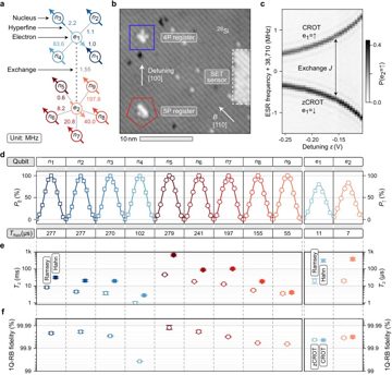
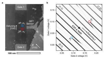
- 11-qubit donor processor Silicon Quantum Computing paper press ▣ Fig. 1b (STM micrograph after hydrogen lithography); §Main (P atoms placed ≲3 nm apart) ✅
Pictures
Every picture carries the story of what it shows and its credit line.

STM hydrogen-resist lithography (donors)
A scanning-tunnelling tip desorbs hydrogen from passivated Si(100) to open single sites, phosphine dopes them, and epitaxial silicon buries the donors — atom-precise, serial, and without a foundry equivalent.
Verdict. Eleven qubits at atom precision prove the physics; with one practitioner, no merchant tool and no published parallel-write scheme, this stays a boutique process whatever the 2033 target says.
Λ = error-suppression factor per code-distance step; QBI = DARPA Quantum Benchmarking Initiative (Stage A concept → B R&D plan → C government V&V); G1–G7 = the report's goal classes (see Actors & economics).
Identity & lineage
A hydrogen-terminated Si(100) surface is the resist. The tip removes hydrogen from selected dimers by electron-stimulated desorption; phosphine adsorbs only on the bare silicon; an anneal incorporates phosphorus substitutionally; low-temperature epitaxy buries the result. Hydrogen-resist patterning predates its qubit use by two decades; UNSW's Simmons group made a single-atom transistor in 2012 D[357] and SQC — branding the flow PAQMan — an 11-qubit processor in 2025 D[192].
Attributes: engineered placement of a natural dopant, no mobility and no control step, Pauli error once fabricated, a fabrication class with no CMOS analogue.
Physics & limits
Throughput is the floor, structurally: one tip visits one site at a time, so the process scales as O(N) in qubits where photolithography scales as O(1) in wafers. In-plane registration inside the desorption window is near a lattice constant, but the donor's final position carries ~3 nm of uncertainty from segregation and diffusion during incorporation and encapsulation: the limiting step is thermal, not lithographic. Encapsulation temperature is the real trade: hot enough for good epitaxy moves donors, cold enough to freeze them leaves defects that dephase the electron. Only parallel exposure changes the scaling law.
Engineering state of the art
table
Dominant term: device count. Every STM-donor device is fabricated individually; no parallel process exists at any scale and no placement-yield distribution is published.
Not published: a primary measurement of the incorporated-donor position distribution behind the ~3 nm placement precision; the amounts of the Firgun Ventures investment, the SkyWater agreement and the AMD collaboration, and the split of the A$60 M NRFC total by tranche; a parallelisation scheme for STM donor placement, by SQC or any other group; and any SQC statement on IonQ's acquisition of SkyWater.
Manufacturing, materials & supply chain
No vendor sells a turnkey donor-placement tool: the equipment (UHV STM, phosphine handling, epitaxy) is merchant, the recipe is not, so no second source can be procured. Feedstock is no longer scarce: enriched ²⁸Si from ASP Isotopes and, from 2026-07-16, US DOE silane at 99.9999% ²⁸Si P[348]. SkyWater supplies US resonators and packaging (2025-11-20) C[276], and IonQ, a competing platform vendor, closed its ~USD 1.8 B acquisition of SkyWater on 2026-07-31 G[19] — the sharpest supply risk here. Export control bites on the feedstock, not the tool: no Export Control Classification Number (ECCN) covers STM lithography, but the US rule of 2024-09-06 created ECCNs for isotopically enriched silicon and germanium — silicon qualifies below 0.08% of the nuclear-spin isotope ²⁹Si — as epitaxial layers (3C907), hydrides such as silane (3C908) and bulk material or oxide (3C909), which takes in the DOE silane; its quantum-computer ECCN, 4A906, starts at 34 qubits and, below 2,000, applies only under a two-qubit (C-NOT) error ceiling set for each size band — out of reach of an eleven-qubit device G[301]. Burden at scale is unknown — no device beyond eleven qubits exists.
Role in the stack
The manufacturing layer of donor spins in silicon: provides the donor-spin carrier and, through it, hyperfine-gated registers and spin-to-charge readout; it substitutes for foundry CMOS at placement, trading wafer throughput for unmatched precision. Nothing else in the stack requires it — the strategic weakness: a defect here cannot be routed around, and no other node gains from progress on it. Verification: the 11-qubit fidelities come from one paper by the only group practising the process D[192] — no second fabricator, and three fidelity framings across preprint, journal and main report.
Actors & economics
Who.
| Organisation | Role | Country | What exactly they do | Evidence |
|---|---|---|---|---|
| SQC | developer | Australia | Sole practitioner of STM donor placement | D[192] |
| SkyWater Technology | supplier | USA | Resonators and packaging | C[276] |
| IonQ | supplier | USA | Owns SkyWater since 2026-07-31 | G[19] |
| NVIDIA | supplier | USA | NVQLink interconnect, SQC among 17 builders | C[531] |
| AMD | supplier | USA | Hardware for qubit control and readout, and compute for simulation (collaboration announced 2026-04-07) | C[358] |
Money. 2025-11-06 · SQC · QBI Stage B · up to USD 15 M · DARPA · awarded fact. 2026-03-24 and 2026-06-11 · SQC · equity · A$60 M combined · Australia's NRFC · closed fact. 2026-06-11 · SQC · investment · undisclosed · Firgun Ventures · announced C[358]. 2026-07-31 · IonQ · acquisition of supplier SkyWater · ~USD 1.8 B · closed G[19].
Market & supply chain. There is no market: one operator, no merchant process. Cost per placed donor is unpublished, so unit economics cannot be checked against the 2033 target. Funds G2 and G3; G4 needs parallelisation that does not exist.
IP & standards. Foundational patents trace to the UNSW/Simmons line; no dated family count from a named database as of 4 Sep 2026, and no standard covers atom-precision placement.
Roadmaps & track record. SQC (2026-06 · commercial scale by 2033 Rfact · unmet, eleven qubits published). "Continuous scaling" and "a million qubits" appear in company material with no published mechanism C[358], so the target is unfalsifiable rather than ambitious.
Strategic reading. If a parallel-write scheme appears, a decade of recipe knowledge compounds into a real moat. Without one, the precision that makes the process attractive is what caps it, and value migrates to whoever puts donors in a foundry flow.
Outlook & open questions
Confirm/demote (12–24 months): a dated parallel-fabrication announcement or a device beyond eleven qubits confirms a path past boutique scale; neither by 2028 demotes this to a physics tool. Best case 2029: above fifty donors with published yield. Worst case: a single-laboratory capability. Open: (1) is multi-tip or templated exposure feasible; (2) does SkyWater's new owner keep the relationship; (3) does anyone publish a placement-yield distribution.
References
- [19] IonQ, “IonQ Completes Acquisition of SkyWater Technology,” Jul. 31, 2026. [Online]. Available: https://www.ionq.com/
news/ Gionq-completes-acquisition-of-skywater-technology - [192] H. Edlbauer et al., “An 11-qubit atom processor in silicon,” Nature, vol. 648, no. 8094, pp. 569–575, Dec. 2025, doi: 10.1038/s41586-025-09827-w. arXiv:2506.03567. D
- [276] Silicon Quantum Computing, “SkyWater x SQC: Advancing Hybrid Quantum-Classical Computing,” Nov. 20, 2025. [Online]. Available: https://sqc.com/
news/ Cskywater-and-sqc-advancing-hybrid-quantum-classical-computing - [301] US Department of Commerce, Bureau of Industry and Security, “Commerce Control List Additions and Revisions; Implementation of Controls on Advanced Technologies Consistent With Controls Implemented by International Partners,” Federal Register, vol. 89, p. 72926, Sep. 6, 2024. [Online]. Available: https://www.federalregister.gov/
documents/ G2024/ 09/ 06/ 2024-19633/ commerce-control-list-additions-and-revisions-implementation-of-controls-on-advanced-technologies - [348] U.S. Department of Energy, “DOE Advances Domestic Supply of Silicon, Germanium Isotopes for Quantum Computing,” HPCwire, Jul. 16, 2026. [Online]. Available: https://www.hpcwire.com/
off-the-wire/ Pdoe-advances-domestic-supply-of-silicon-germanium-isotopes-for-quantum-computing/ - [357] M. Fuechsle et al., “A single-atom transistor,” Nat. Nanotechnol., vol. 7, no. 4, pp. 242–246, Apr. 2012, doi: 10.1038/nnano.2012.21. D
- [358] Silicon Quantum Computing, “Silicon Quantum Computing — News,” sqc.com. [Online]. Available: https://sqc.com/
news/ C - [531] NVIDIA, “NVIDIA Introduces NVQLink — Connecting Quantum and GPU Computing for 17 Quantum Builders and Nine Scientific Labs,” Oct. 28, 2025. [Online]. Available: https://nvidianews.nvidia.com/
news/ Cnvidia-nvqlink-quantum-gpu-computing