Diamond growth / implantation (NV, SiV, SnV) fab_diamond
Plasma CVD growth of single-crystal diamond, ion implantation and annealing to form NV, SiV or SnV centres, and undercut etching to build the nanophotonics around them.
Diamond growth / implantation (NV, SiV, SnV)
SnV nanocavities (QuTech, PRX 2026): 327 characterised at room temperature on two chips, coupled centres in 7 of 9 cooled, two measured above cooperativity one — no chip-wide yield published; Quantum Brilliance diamond foundry.
Brief →Key references
Design space — attributes
- (a) carrier affinity
- intermediate / carrier-agnostic
- (b) time · entangling
- —
- (c) readout
- —
- (d) mobility
- —
- (e) control
- —
- (f) error structure
- stochastic Pauli
- (g) manufacturing
- diamond growth / implantation
Evaluation space — dated attributes
Element Six's DNV-B1 (2020) is an NV-*ensemble* sensing grade, not a substrate for single-defect network nodes, which need electronic-grade plates.
Standard records
Actors & goals — annotations
Edges
Used by 4 machines (4 primary · 0 alternate)
- defect spins 4
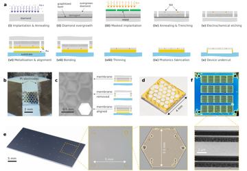
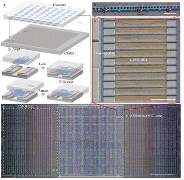
- Diamond-spin quantum computer prototype Fujitsu (with TU Delft and QuTech) press ▨ Overview of developed technologies: heterogeneous material bonding and thinning; PIC fabrication for SnV centres ✅
- Quoll / QB-QDK 2.0 Quantum Brilliance press ▨ ✅
- QC2026 Dual Core SaxonQ press ◌ 🔎
- SXQ4 SaxonQ product page ◌ 🔎
Pictures
Every picture carries the story of what it shows and its credit line.

Diamond growth / implantation (NV, SiV, SnV)
Plasma CVD growth of single-crystal diamond, ion implantation and annealing to form NV, SiV or SnV centres, and undercut etching to build the nanophotonics around them.
Verdict. Two independent lotteries — where the ion stops and how the cavity lands on it — set device yield, and nobody publishes it: QuTech characterised 327 SnV cavities at room temperature, found coupled centres in 7 of the 9 it cooled, and measured two above cooperativity one.
Λ = error-suppression factor per code-distance step; QBI = DARPA Quantum Benchmarking Initiative (Stage A concept → B R&D plan → C government V&V); G1–G7 = the report's goal classes (see Actors & economics).
Identity & lineage
Plasma CVD grows single-crystal diamond on a seed; nitrogen, silicon or tin is implanted; a high-temperature anneal mobilises vacancies that bind the impurity into a colour centre; the optical structure is then cut from the bulk. That last step is the defining constraint: there is no diamond-on-insulator wafer and no sacrificial layer, so cavities are released by undercut etching of the same crystal that hosts the defect. Implantation-based fabrication matured around 2010; QuTech's 2026 SnV cavity study sets the benchmark Dfact.
Attributes: engineered placement of a natural defect, no mobility and no control step, Pauli error once fabricated, diamond fabrication with no CMOS analogue.
Physics & limits
Three independent things must go right at one site. The ion must stop where intended: straggle is tens of nanometres, an order worse than STM donor placement. It must convert into an optically good centre — only a fraction take the wanted charge state, and residual damage broadens the line. Then the etched cavity must put its field maximum on that centre: cooperativity goes as g²/κγ, with g set by position inside a mode a few hundred nanometres across. The three partial yields multiply, and none is published over a whole chip: of 327 cavities characterised at room temperature, 9 were cooled, 7 of them held a coupled SnV, and the two measured in full reached coherent cooperativity 8.3 and 1.6 Dfact. Only deterministic single-ion implantation with event detection, or in-growth delta doping with registration, moves that floor; neither exists at device scale.
Engineering state of the art
table
| year | figure | who | tag+key |
|---|---|---|---|
| 2024-05-15 | implanted SiV nanophotonic nodes at 0.69(7) over 35 km of fibre | Harvard | D[209] |
| 2025-11-27 | fibre microcavity around a bulk NV raises collection ~0.05% → ~0.5% | QuTech | D[359] |
| 2026-06 | 327 SnV nanocavities on two chips, mean Q 1.1×10⁴ at room temperature; coupled centres in 7 of 9 cooled; coherent cooperativity up to 8.3 | QuTech | Dfact |
Dominant term: device yield. The fibre microcavity is a fabrication answer as much as an optical one: the resonator sits outside the crystal, removing the undercut-etch lottery.
The 327-cavity SnV study, first reported in a news item [362], is published in Physical Review X fact: its 327 cavities were characterised at room temperature, only 9 were cooled, and the two emitter–cavity devices measured in full exceeded cooperativity one; the result is single-source and unreplicated. Its ¹²⁰Sn implant at 350 keV reaches a depth of 88 ± 16 nm fact, a spread of tens of nanometres. Element Six's lead as the diamond source of most NV-centre companies rests on a secondary survey [364]. Not published: the fraction of the 327 cavities above cooperativity one, so device yield is unknown; the lateral implantation straggle and an ion-to-usable-centre conversion yield; a dated capacity, revenue or investment figure for Element Six's quantum segment; and a cost per device, wafer count or throughput for any diamond quantum process.
Manufacturing, materials & supply chain
Element Six is the main merchant supplier, selling plates by catalogue; its DNV-B1 grade (2020-06-15) targets NV ensembles, while single-defect work needs electronic-grade single crystal C[361]. Its growth capacity sits in the UK and California C[361]; two smaller sources are Diatope, an Ulm University spin-out (2021) selling engineered NV diamond, and Quantum Brilliance's quantum-diamond foundry in Melbourne, opened in 2025 to make quantum-grade diamond at scale P[364]. Implantation runs on general-purpose accelerators; ¹²C-enriched growth costs more. Nothing is on a 300 mm path: millimetre-scale plates processed individually, with no published wafer count, cost or throughput. Export exposure is not nil: since 2022-08-15 the US Export Control Classification Number (ECCN) 3C005.a names diamond semiconductor substrates, ingots and boules above 10⁴ Ω·cm, and 3C006 an epitaxial diamond layer on such a substrate fact; whether an electronic-grade quantum plate counts as a semiconductor substrate has not been ruled on, and no ECCN names colour centres. Burden passed upward: a laser and a detector per site.
Role in the stack
Provides the host crystal colour-centre spins and their gates require, hence the defect-node architecture. It is the counterpart of STM hydrogen-resist lithography, not a substitute: implantation buys area throughput at an order of magnitude of placement precision, and neither route publishes a yield distribution. Verification: the 327-cavity study is one institution's, announced in a news release P[362] and peer-reviewed in Physical Review X Dfact, with nothing to replicate it against.
Actors & economics
Who.
| Organisation | Role | Country | What exactly they do | Evidence |
|---|---|---|---|---|
| QuTech | research | Netherlands | SnV nanocavity fabrication and cryogenic characterisation | Dfact |
| Element Six | supplier | UK | Merchant CVD diamond plates | C[361] |
| Diatope | supplier | Germany | Engineered NV diamond; Ulm University spin-out (2021) | P[364] |
| Harvard | research | USA | Implanted SiV nanophotonics | D[209] |
| Quantum Brilliance | developer | Australia | Room-temperature units; quantum-diamond foundry in Melbourne (2025) | P[364] |
| QuantumDiamonds | developer | Germany | NV microscopy, Munich | P[364] |
Money. 2026-07 · QuantumDiamonds · grant and equity · EUR 91 M, EUR 76 M of it EU Chips Act · financing a EUR 152 M Munich facility · closed P[364]. 2025-01 · Quantum Brilliance · Series A · USD 20 M · ~USD 58 M cumulative · closed P[364]. No QBI stage names diamond manufacturing.
Market & supply chain. One dominant substrate supplier is the concentration risk, its two alternatives dating only from 2021 and 2025; accelerators and etch tools are generic. Unit economics are unpublished. Pays into G6 and sensing.
IP & standards. No dated patent family from a named database as of 4 Sep 2026; Element Six's DNV grades are a de facto benchmark.
Roadmaps & track record. QuTech (modular-computing programme · on schedule) P[362]. QuantumDiamonds (Munich facility, 2026-07 · too new to judge) P[364]. Quantum Brilliance (units at three laboratories · delivered, dates unstated) P[364]. No actor publishes a dated yield target.
Strategic reading. Element Six wins in every scenario: it sells substrate to actors who compete with each other, not it. The fibre microcavity is the quiet threat — a resonator outside the crystal removes most of the nanofabrication problem.
Outlook & open questions
Confirm/demote (12–24 months): deterministic single-ion implantation with event detection, or a published chip-wide fraction of cavities above cooperativity one, confirms; two more years without either demotes this to a research process. Best case 2029: chip-scale arrays with tens of usable nodes. Worst case: every node stays hand-selected. Open: (1) can implantation precision approach one nanometre; (2) do Diatope or Quantum Brilliance's foundry grow into a second source at Element Six's scale; (3) does external-cavity coupling displace monolithic nanophotonics.
References
- [209] C. M. Knaut et al., “Entanglement of nanophotonic quantum memory nodes in a telecom network,” Nature, vol. 629, no. 8012, pp. 573–578, May 2024, doi: 10.1038/s41586-024-07252-z. D
- [359] J. Fischer et al., “Spin-photon correlations from a Purcell-enhanced diamond nitrogen-vacancy center coupled to an open microcavity,” Nat. Commun., vol. 16, no. 1, Art. no. 11680, Nov. 2025, doi: 10.1038/s41467-025-66722-8. D
- [361] Element Six, “Element Six launches DNV-B1™ – its first commercially-available, general-purpose quantum grade diamond,” Jun. 15, 2020. [Online]. Available: https://www.e6.com/
en/ Cabout/ news/ dnv-b1-launch - [362] QuTech, “Coherent coupling of diamond colour centre to a nanocavity,” Jun. 25, 2026. [Online]. Available: https://qutech.nl/
2026/ P06/ 25/ a-step-toward-faster-quantum-networks/ - [364] M. U. Rehman, “Top Diamond NV-Centre Quantum Computing Companies in 2026,” The Quantum Insider, Jul. 10, 2026. [Online]. Available: https://thequantuminsider.com/
2026/ P07/ 10/ 8-quantum-computing-companies-working-with-nv-centre-in-diamond-technology/