Electro-optic drive + feed-forward electronics (room temperature) ct_eo
Room-temperature modulators driven from detector outcomes inside one optical clock cycle — the feed-forward layer every photonic architecture needs.
Electro-optic drive + feed-forward electronics (room temperature)
MHz–GHz switching of BTO/TFLN modulators conditioned on detector outcomes within one clock cycle.
Brief →Key references
Design space — attributes
- (a) carrier affinity
- photon (natural particle, engineered modes)
- (b) time · entangling
- —
- (c) readout
- —
- (d) mobility
- —
- (e) control
- electro-optic @ room temperature
- (f) error structure
- loss (erasure)
- (g) manufacturing
- photonic IC foundry
Evaluation space — dated attributes
Standard records
Actors & goals — annotations
Edges
Used by 14 machines (14 primary · 0 alternate)
- photonics 14
- ETRI 8-photon silicon-photonic qubit chip ETRI (with KAIST and the University of Trento) paper ◌ 🔎
- PT-1 ORCA Computing paper product page ▦ 🔎
- PT-2 ORCA Computing product page press ▦ 🔎
- Omega chipset (Moreton Bay / Chicago systems unnamed) PsiQuantum paper product page press ▣ Fig. 5d–g (BTO Pockels, phase shifter); §Electro-optic switching ✅
- Belenos Quandela product page press ▣ §II Chip control; SI §S-IV + Fig. S8 (phase-shifter voltage model) ✅
- Quandela Canopus Quandela product page product page press ◌ 🔎
- Lucy Quandela press ▦ 🔎
- Carina QuiX Quantum ▨ ✅
- Jiuzhang (1.0) USTC (Pan Jianwei group) press ◌ 🔎
- Jiuzhang 2.0 USTC (Pan Jianwei group) paper press ▤ 🔎
- Jiuzhang 3.0 USTC (Pan Jianwei group) paper press ◌ 🔎
- Jiuzhang 4.0 USTC (Pan Jianwei group) paper press ▣ Extended Data Fig. 4 (schematic of the phase locking system); Extended Data Fig. 1 (PZT-stabilised MZI) ✅
- Aurora Xanadu paper press link ▣ Fig. 2 (four-rack system modules); Extended Data Fig. 1 (hardware block diagram) ✅
- Borealis Xanadu paper link ▤ Experiment (demux: 15 low-loss resonant EOMs in 4 layers -> 16 detector channels) 🔎
Pictures
Every picture carries the story of what it shows and its credit line.
Electro-optic drive + feed-forward electronics (room temperature)
Room-temperature modulators driven from detector outcomes inside one optical clock cycle — the feed-forward layer every photonic architecture needs.
Verdict. Loop latency reached 150–196 ns in 2026 against an 80 ns switch: electronics sit ~2× above the component floor, not orders of magnitude. Demote if no system-scale sub-µs loop by 2028.
Λ = error-suppression factor per code-distance step; QBI = DARPA Quantum Benchmarking Initiative (Stage A concept → B R&D plan → C government V&V); G1–G7 = the report's goal classes (see Actors & economics).
Identity & lineage
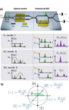
The 300 K layer that drives photonic qubits and closes the measurement loop: pump lasers, thin-film lithium-niobate (TFLN) or barium-titanate (BTO) modulators, and electronics turning a detector click or homodyne quadrature into a drive voltage before the next photon arrives. Alone among control nodes it has no cryogenic variant: electronics at 300 K read detectors near 2 K, so every loop crosses that boundary twice. Attributes: no carrier of its own, immobile, loss-dominated error; electro-optic modality at room temperature, photonic-IC fabrication.
Physics & limits
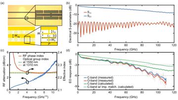
Modulator bandwidth is not the constraint. What binds is detector rise, discrimination, decision and driver settling, which must fit inside optical delay you can afford. Holding a photon 100 ns in silicon nitride costs ~15 m of waveguide; at PsiQuantum's measured 1.8 ± 0.2 dB/m single-mode SiN loss that is ~27 dB against a per-photon budget near 0.5 dB. The same delay in fibre costs ~4 mdB plus two fibre-to-chip transitions at 52 ± 12 mdB D[169]. Feed-forward delay must live off-chip; its loss price is packaging, not waveguide S. Past ~1 GHz the wall becomes SNSPD dead time.
Engineering state of the art
table
June 2026 reset the arithmetic: 80 ns against a 1 µs cycle is ~12×, and rack electronics at 150–196 ns cut it to ~2×. That array's zero static power costs 1.48 dB per cell, ~15× PsiQuantum's 100 mdB in-line switch D[169], [516] — routing plane, not fusion plane.
The three 2026 latency figures sit at different reference planes, and no source reconciles them. The 27 dB on-chip against 4 mdB in-fibre delay comparison is derived from published loss figures, not measured. Not published: a cost per modulator or per feed-forward channel.
Manufacturing, materials & supply chain
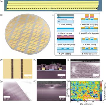
TFLN comes from two merchant vendors, HyperLight and Lightium P[518]; volume BTO only from PsiQuantum's 300 mm GlobalFoundries flow D[169] and Lumiphase's pilot D[516]; Xanadu's 0.085 dB/facet coupling used Corning and DISCO C[172]. No cost per channel is public. I/O burden is this node: a driver and DAC per modulator, a coax and discriminator per detector. QuiX's unit is 32×32 C[825], so 10³ modes is ~30 racks; at 10⁴ the wall is inter-rack clock skew, at 10⁶ nothing scales. The machine falls under BIS ECCN 4A906 fact.
Role in the stack
Shared, not an architecture choice: it drives the fusion architecture (PsiQuantum, Quandela, QuiX) and the continuous-variable/GKP architecture (Xanadu) identically, also serves the boson sampler, and sets the derived clock wherever fusions or homodyne measurements iterate — 1.0 MHz at system scale, 5–7 MHz at unit scale. Verification: the figures sit at three reference planes. QuiX's ~150 ns is detector-to-drive C[825]; 196 ns a full CV loop P[822]; Aurora's 1 MHz a cycle time, not a latency D[173].
Actors & economics
Who.
| Organisation | Role | Country | What they do | Evidence |
|---|---|---|---|---|
| Xanadu | developer | CA | Only system-scale single-cycle feed-forward | D[173] |
| PsiQuantum | developer | US | 300 mm BTO switches, DARPA V&V | D[169] |
| QuiX Quantum | developer | NL | Rack feed-forward unit, ~150 ns | C[825] |
| Lumiphase | supplier | CH | Non-volatile BTO array | D[516] |
Money.
2024-09 · HyperLight · Series B · USD 37 M · Summit Partners · closed P[518]
2025-07-10 · QuiX · Series A · EUR 15 M · Invest-NL, EIC · closed Cfact
2026-05-21 · GlobalFoundries · CHIPS LOI · USD 375 M · US Commerce fact
2026-07-22 · PsiQuantum · QBI Stage C, BTO-switch V&V · USD 125 M · DARPA P[181]
Market & supply chain. Two TFLN vendors, one volume BTO line, and no merchant vendor of low-latency feed-forward at all — each firm builds its own. The scarce input is the deterministic sub-200 ns detector-to-driver path, not the modulator. Pays for G3/G4, G6.
IP & standards. No feed-forward patent family surfaced from a dated database as of 2026-09-04; the BTO gate array is the dated advance D[516].
Roadmaps & track record. Xanadu 1 MHz (delivered 2025-01, unimproved) D[173]; QuiX named fast feed-forward a 2026 blocker in 2025-07 and installed the unit 2026-06-02 C[825]; PsiQuantum published no 2026 hardware result P[181]. QuiX alone shipped what it named.
Strategic reading. If sub-200 ns loops generalise, the bottleneck migrates to detector dead time and the fibre delay lines holding photons during the decision — favouring owners of packaging and detector supply over FPGA vendors. A merchant feed-forward box would commoditise a layer three firms treat as differentiation.
Outlook & open questions
Confirm by 2027: a loop under 200 ns above 32 channels, or a system cycle faster than 1 MHz; demote if Aurora's 1 MHz still stands in 2028. Best case 2029: ~10 MHz rack-scale. Worst case: unit latency never couples to scale. Open: does 150 ns hold under 32-channel load; does non-volatile BTO reach usable in-line loss.
References
- [169] K. Alexander et al., “A manufacturable platform for photonic quantum computing,” Nature, vol. 641, no. 8064, pp. 876–883, Feb. 2025, doi: 10.1038/s41586-025-08820-7. D
- [172] Xanadu, “Xanadu sets new industry benchmark in photonic chip packaging,” PR Newswire, Jun. 10, 2026. [Online]. Available: https://www.prnewswire.com/
news-releases/ Cxanadu-sets-new-industry-benchmark-in-photonic-chip-packaging-302796562.html - [173] H. A. Rad et al., “Scaling and networking a modular photonic quantum computer,” Nature, vol. 638, no. 8052, pp. 912–919, Jan. 2025, doi: 10.1038/s41586-024-08406-9. D
- [181] M. Abdel-Kareem, “PsiQuantum Secures $125 Million Expanded Agreement with DARPA under QBI Program,” Quantum Computing Report, Jul. 22, 2026. [Online]. Available: https://quantumcomputingreport.com/
psiquantum-secures-125-million-expanded-agreement-with-darpa-under-qbi-program/ P - [516] C. Català-Lahoz et al., “High-speed non-volatile barium titanate field-programmable photonic gate array,” Nat. Photon., vol. 20, no. 8, pp. 932–940, Aug. 2026, doi: 10.1038/s41566-026-01934-y. D
- [518] optics.org, “Lithium niobate in vogue as thin-film developers raise cash,” Sep. 24, 2024. [Online]. Available: https://optics.org/
news/ Plithium-niobate-in-vogue-as-thin-film-developers-raise-cash - [822] D. Duggan et al., “FPGA Based Feedforward System for Photonic Quantum Computing Applications,” arXiv:2606.03500, Jun. 2026. P
- [825] QuiX Quantum, “QuiX Quantum Installs Real-Time Control Component for Universal Photonic Quantum Computer,” Jun. 2, 2026. [Online]. Available: https://www.quixquantum.com/
news/ Cquix-quantum-installs-real-time-control-component-for-universal-photonic-quantum-computer