PIC-generated tweezers / integrated optics for atoms ct_pic_trap
Generating, routing and collecting the light that traps, addresses and images single atoms from a photonic integrated circuit instead of free-space optics.
PIC-generated tweezers / integrated optics for atoms
Trap generation moved onto a photonic chip (4 atoms, 27.5 s lifetimes); fabricated-world optics for a natural carrier.
Key references
Design space — attributes
- (a) carrier affinity
- photon (natural particle, engineered modes)
- (b) time · entangling
- —
- (c) readout
- —
- (d) mobility
- —
- (e) control
- optical @ room temperature
- (f) error structure
- coherent / calibration
- (g) manufacturing
- photonic IC foundry
Evaluation space — dated attributes
Pasqal. Two functions hide here and only the first is trap generation: UChicago's 2024 tweezers are free-space traps over nanophotonic cavities, and USTC's 2026 glass-waveguide chip addresses trapped atoms rather than generating the traps.
Standard records
Actors & goals — annotations
Edges
Used by 3 machines (0 primary · 3 alternate)
- neutral atoms 3
- Pasqal Centaurus Pasqal product page press ▨ 🔎 (alternate)
- Fresnel / Fresnel 2 Pasqal ▨ 🔎 (alternate)
- Pasqal Lyra Pasqal press ▨ 🔎 (alternate)
Pictures
Every picture carries the story of what it shows and its credit line.
PIC-generated tweezers / integrated optics for atoms
Generating, routing and collecting the light that traps, addresses and images single atoms from a photonic integrated circuit instead of free-space optics.
Verdict. Four atoms trapped from a chip, fifty addressed through a chip, zero gates through either. Until a PIC holds atoms far enough from its surface to run Rydberg gates, this is packaging, not a scaling path.
Λ = error-suppression factor per code-distance step; QBI = DARPA Quantum Benchmarking Initiative (Stage A concept → B R&D plan → C government V&V); G1–G7 = the report's goal classes (see Actors & economics).
Identity & lineage
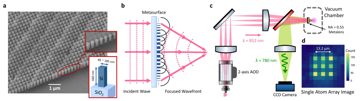
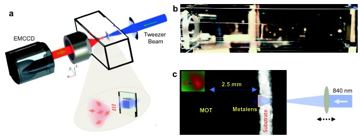
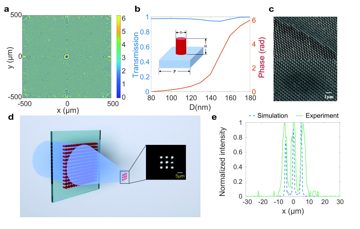
Move the optics that hold and address single atoms — lenses, modulators and deflectors on a metre-scale breadboard — onto a photonic chip. Two functions hide under one node and only the first is trap generation: emitting tweezer light from the chip (Pasqal, four rubidium atoms, ~27.5 s lifetime, August 2026 C[330]), and coupling trapped atoms to on-chip photonics for imaging and collection (Chicago, 64 free-space tweezers over >100 nanophotonic cavities D[579]; a 50-atom, 784-channel glass waveguide array D[580]). Reconfiguring traps on chip, nobody has shown.
Control and fabrication: room-temperature optical control from a photonic IC, wrapping a natural carrier it never becomes. Error structure: coherent — coupling loss, crosstalk (0.4% measured D[580]) and surface-induced light shifts, not decoherence.
Physics & limits
A rubidium tweezer needs roughly a millikelvin of depth: several milliwatts focused to a micron waist at high numerical aperture. A grating or metasurface emitter can do that, and Pasqal's lifetime matches its own bulk systems C[330], so coupling loss is not the first wall. Power is next: a thousand traps is watts on chip, where scattered light and coupler heating bind first.
The first wall is the surface. Rydberg states are enormously polarisable, so adsorbate-induced stray fields and blackbody radiation from a nearby dielectric shift and broaden the line every neutral-atom two-qubit gate depends on. Chicago holds atoms a few hundred nanometres above the chip for cavity coupling D[579] — excellent for photon collection, hopeless for a blockade gate. A trap-generating chip must project its focus tens to hundreds of microns clear of itself, spending much of the footprint advantage. The second wall is reconfiguration: crossed deflectors sweep continuously and are already the bandwidth limit above ~10⁴ atoms, while on-chip switching is thermo-optic (microseconds to milliseconds, milliwatts dissipated each) or electro-optic in lithium niobate (nanoseconds, lossier, not trap-grade yet). What moves the floor: surface passivation letting atoms sit closer, and a low-loss switch fabric beating deflector rates.
Engineering state of the art
table
| Year | Figure | Who | Tag+key |
|---|---|---|---|
| 2024-07 | 64 tweezers over >100 nanophotonic cavities, 99.2% imaging fidelity, atoms a few hundred nm above the surface | University of Chicago | D[579] |
| 2026-08 | 4 Rb atoms trapped by light from a SiN chip, ~27.5 s lifetime, stated as matching bulk optics | Pasqal | C[330] |
| 2026-08 | 50 addressed ⁸⁷Rb atoms through a glass waveguide array: 0.4% crosstalk, 2.9 dB insertion loss, 93% fill, 118 Hz loss repair, 784-channel chip | USTC | D[580] |
Two to three orders below free-space systems on atom count, and no gate or transport has run through a chip-generated trap anywhere. The 784-channel chip is the strongest scaling evidence, and it addresses atoms rather than trapping them.
On the light-source side, a hybrid-integrated 780 nm microcomb (Si₃N₄ resonators from 150 mm wafers, self-injection-locked III–V laser diodes) referenced to ⁸⁵Rb drove an optical lattice and a Raman coupling in an ⁸⁷Rb Bose–Einstein condensate in 2026 P[886]. The light was chip-generated but delivered through free space, and it controlled a quantum gas, not qubits: no chip-generated trap or gate was involved.
Manufacturing, materials & supply chain
Silicon nitride photonic-IC processes; the 50-atom array uses glass waveguides D[580]. Pasqal's photonics came from Aeponyx at an undisclosed price under 18 months before the August 2026 release, and no foundry partner is named C[581]. Nearest merchant capacity: imec's PIXEurope pilot line (~EUR 400 M, 2024-11-24) and GlobalFoundries' Quantum Technology Solutions ($375 M CHIPS letter of intent, 2026-05-21) — both name photonics as an output, neither names atom traps G[582]G[353]. Thin-film lithium niobate vendors HyperLight and Lightium are the candidates if fast switching becomes the requirement P[518]. No yield, per-channel cost or export-control category for atom-trap photonics was found as of 2026-09-04.
Control, readout & I/O burden
The claim is footprint: Pasqal states up to 50× smaller optics once trap light is routed on chip C[330]. At four atoms the burden is a few fibre couplings; the question starts at hundreds, where it becomes power per channel, fibre count into vacuum and switching bandwidth — none of which is published. The 784-channel chip at 2.9 dB insertion loss is the only channel-count datum D[580]. A chip removes an optical table's alignment and drift burden and adds a fixed geometry unless switches are integrated.
Role in the stack
It replaces free-space tweezer and addressing optics on the alkali neutral-atom architecture (Pasqal, QuEra, Infleqtion) and requires a photonic-IC process underneath, providing no connectivity, gate or code of its own. Contribution to the derived clock is nil today; at scale, on-chip switching could become a new clock term if it cannot match deflector reconfiguration — the opposite of the intended effect. The same pattern runs on the ion side, where Sandia supplies Quantinuum integrated photonics for laser delivery G[501]. Neighbouring empty slots: a gate through a chip-generated trap, and on-chip transport.
Evidence — how the numbers were measured
Pasqal's lifetime and 50× footprint projection are company-reported without replication, and "matching bulk optics" is measured against its own systems, not an external reference C[330]. The Chicago and USTC results carry no vendor roadmap and neither reports a gate fidelity, because neither has run a gate. Nothing published measures what matters most — trap depth, position stability and Rydberg-line shift against distance from the chip surface.
The millikelvin trap depths and milliwatt-per-trap powers are standard tweezer scalings, not values quoted by the chip sources. Not published: the Aeponyx acquisition price and closing date (only "less than 18 months" before 2026-08-10 is stated); the numbers behind Pasqal's 50× footprint projection; and the yield, per-channel cost and export-control classification of atom-trap photonics.
Actors & economics
Who.
| Organisation | Role | Country | What they do here | Evidence |
|---|---|---|---|---|
| Pasqal | developer | FR | Only chip-generated atom traps demonstrated | C[330] |
| Aeponyx | supplier | CA | SiN photonics behind Pasqal's chip; acquired | C[581] |
| University of Chicago | research | US | Atom array over nanophotonic cavities, background-free imaging | D[579] |
| USTC | research | CN | 50-atom addressing array, 784-channel chip | D[580] |
| GlobalFoundries | supplier | US | Quantum unit naming photonics as an output | G[353] |
| HyperLight | supplier | US | Lithium niobate for fast switching | P[518] |
Money. 2024-09 · HyperLight and Lightium · Series B and seed · $37 M and $7 M · Summit Partners; Vsquared and Lakestar · closed Pfact. 2025 (undated) · Pasqal · M&A of Aeponyx · undisclosed · closed, stated as under 18 months before 2026-08 C[581]. 2026-08-28 · Pasqal · SPAC merger · ~$360 M cash · Nasdaq PSQL · closed fact.
Market & supply chain. The supply base is the general photonic-foundry ecosystem, not scarce; the scarce asset is trap design know-how, and Pasqal's arrived with one acquired startup — a single point of failure if that team disperses. What it threatens is the incumbent free-space chain: deflectors from AA Opto-Electronic and Gooch & Housego, the only vendors named in published tweezer work D[4]. It pays for G3 and G4 by cutting footprint and alignment labour, nothing for G1, G2 or G5.
IP & standards. Aeponyx's pre-acquisition silicon-nitride portfolio is the core asset; Pasqal has disclosed nothing of its contents. No dated patent-family count for chip-generated atom tweezers was found as of 2026-09-04, and no standards activity addresses trap-grade photonics.
Roadmaps & track record. Pasqal states >10,000 atoms and 100 logical qubits by this route with no date attached R[330], against one slip already on the free-space side — 10,000 physical moved from 2026 to 2028, 100 logical to 2029 R[156]fact. First demonstration August 2026: no delivery record to score, and no rival chip-trap roadmap exists.
Strategic reading. If on-chip generation scales past the dozens it undercuts the free-space chain every tweezer and ion machine depends on and moves bargaining power to photonic foundries selling into datacom volumes; Pasqal wins by leading in a component competitors must then buy or build. If crosstalk, power and the surface problem cap channel counts in the tens, it stays packaging and the incumbent vendors keep their position — the likelier outcome on today's evidence.
Outlook & open questions
Confirm/demote in 12–24 months: anyone runs a two-qubit gate through a chip-generated trap; chip-trapped atom count reaches the hundreds; a second vendor enters. Best case 2029: chip tweezers hold hundreds to thousands of atoms at free-space fidelity, shrinking a rack enough to change system cost. Worst case: the surface constraint forces long working distances, the footprint gain evaporates, and integrated optics stays confined to imaging and collection, where it already works. Open: how far from the chip must atoms sit for a clean Rydberg line; can on-chip switching beat deflector reconfiguration. Watch: Pasqal's next update and any gate through a chip trap.
References
- [4] D. Bluvstein et al., “A fault-tolerant neutral-atom architecture for universal quantum computation,” Nature, vol. 649, no. 8095, pp. 39–46, Nov. 2025, doi: 10.1038/s41586-025-09848-5. arXiv:2506.20661. D
- [156] M. Swayne, “Pasqal Completes SPAC Merger With $360 Million in Cash,” The Quantum Insider, Aug. 28, 2026. [Online]. Available: https://thequantuminsider.com/
2026/ R08/ 28/ pasqal-completes-spac-merger-with-360-million-in-cash/ - [330] Pasqal, “Pasqal brings qubit control on-chip, advancing the path to fault-tolerant quantum computing at scale,” Aug. 10, 2026. [Online]. Available: https://www.pasqal.com/
news/ Cpasqal-brings-qubit-control-on-chip-advancing-the-path-to-fault-tolerant-quantum-computing-at-scale/ - [353] GlobalFoundries, “GlobalFoundries launches Quantum Technology Solutions to scale U.S. quantum manufacturing,” May 21, 2026. [Online]. Available: https://gf.com/
gf-press-release/ Also https://investors.gf.com/globalfoundries-launches-quantum-technology-solutions-to-scale-us-quantum-manufacturing/ news-releases/ . Gnews-release-details/ globalfoundries-launches-quantum-technology-solutions-scale-us - [501] T. Rummler, “In the Mountain West, a quantum computing collaboration announces major results,” Sandia Lab News, Aug. 27, 2026. [Online]. Available: https://www.sandia.gov/
labnews/ G2026/ 08/ 27/ in-the-mountain-west-a-quantum-computing-collaboration-announces-major-results/ - [518] optics.org, “Lithium niobate in vogue as thin-film developers raise cash,” Sep. 24, 2024. [Online]. Available: https://optics.org/
news/ Plithium-niobate-in-vogue-as-thin-film-developers-raise-cash - [579] S. G. Menon, N. Glachman, M. Pompili, A. Dibos, and H. Bernien, “An integrated atom array–nanophotonic chip platform with background-free imaging,” Nat. Commun., vol. 15, no. 1, Art. no. 6156, Jul. 2024, doi: 10.1038/s41467-024-50355-4. D
- [580] Y.-D. Hu et al., “A scalable chip-integrated single-photon source array based on 50 individually addressable neutral atoms,” arXiv:2608.15637, Aug. 2026. D
- [581] M. U. Rehman, “Pasqal Demonstrates Photonic Chip-Based Control for Neutral-Atom Quantum Computers,” The Quantum Insider, Aug. 10, 2026. [Online]. Available: https://thequantuminsider.com/
2026/ C08/ 10/ pasqal-photonic-chip-control-neutral-atom-quantum-computers/ - [582] imec, “The European Commission and Chips JU select the PIXEurope consortium to lead the European Pilot Line on Advanced Photonic Integrated Circuits,” Nov. 24, 2024. [Online]. Available: https://www.imec-int.com/
en/ Gpress/ european-commission-and-chips-ju-select-pixeurope-consortium-lead-european-pilot-line - [886] W. Sun et al., “A photonic integrated comb engine for ultracold quantum gases,” arXiv:2609.28294, Sep. 2026. P