Multi-die packaging in one module (flip-chip, bump-bonded control die) ic_multidie
A qubit die bump-bonded face to face with a second superconducting die that carries wiring, resonators, a second material or control logic, inside one package, across a vacuum gap of a few to ~20 µm.
Multi-die packaging in one module (flip-chip, bump-bonded control die)
A qubit die flip-chipped to a wiring or control die inside one package — Sycamore, Zuchongzhi, Ocelot, the SFQ flip-chip module: the interconnect below the module scale, which the multi-chip-module node does not cover.
Brief →Key references
Design space — attributes
- (a) carrier affinity
- fabricated
- (b) time · entangling
- —
- (c) readout
- —
- (d) mobility
- static nearest-neighbour wiring
- (e) control
- microwave @ millikelvin stage
- (f) error structure
- coherent / calibration
- (g) manufacturing
- superconducting lithography
Evaluation space — dated attributes
no dated attribute
Bump yield and thermal mismatch are the limits; it moves the I/O wall, not the module wall.
Actors & goals — annotations
Edges
Used by 12 machines (12 primary · 0 alternate)
- superconducting circuits 12
- Academia Sinica 20-qubit superconducting quantum computer Academia Sinica press ▨ 🔎
- AWS Ocelot AWS Center for Quantum Computing ▤ App. A (Device fabrication) ✅
- WACQT quantum computer (Chalmers 25-qubit flip-chip processor) Chalmers University of Technology (WACQT) ▤ abstract ✅
- Tianyan-287 China Telecom Quantum Group / QuantumCTek / CAS paper docs docs ▤ 🔎
- Sycamore Google Quantum AI paper ▤ §Building a high-fidelity processor (indium bump-bonds between two Si wafers); SI Fig. S1 (packaged chip) ✅
- Sycamore-class 72-qubit processor Google Quantum AI paper paper ◌ 🔎
- IBM Quantum Eagle r1-r3 IBM paper paper paper ▦ O. Dial, 23 Mar 2022, §packaging ✅
- QpiAI Kaveri QpiAI press ▨ 🔎
- SEEQC SFQ-controlled 5-qubit system SEEQC paper press ▤ Supp. §A Device Design and Fabrication ✅
- SUSTech four-dual-rail-qubit processor Southern University of Science and Technology (Huang et al.) paper paper ▣ §II, Fig. 1a; Supplementary §I ✅
- Zuchongzhi 3.0 USTC / Hefei National Laboratory paper paper press ▣ Fig. 1a (two sapphire chips, flip-chip) ✅
- Zuchongzhi 3.2 USTC / Hefei National Laboratory ▤ 🔎
Pictures
Every picture carries the story of what it shows and its credit line.
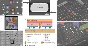
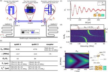
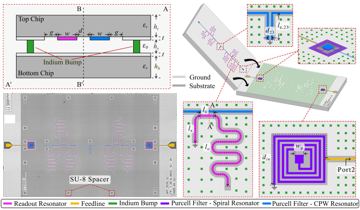
Multi-die packaging in one module (flip-chip, bump-bonded control die)
A qubit die bump-bonded face to face with a second superconducting die that carries wiring, resonators, a second material or control logic, inside one package, across a vacuum gap of a few to ~20 µm.
Verdict. Seven of the register's twelve carriers document a two-die stack in a source that was opened and checked (✅); it moves the wiring wall onto a second die but joins no modules, and as of 2026-09-30 no carrier has published bump yield — Chalmers alone has published a bump count and a gap spread.
In = indium; TSV = through-silicon via; SFQ = single flux quantum, digital superconducting logic; T1, T2,echo = relaxation and echoed dephasing times; Q = quality factor; G1–G7 = the report's goal classes (see Actors & economics).
Identity & lineage
Two superconducting dies face each other across a vacuum gap, joined by indium bumps: one carries the qubits, the other wiring, resonators, another material or control logic — the interconnect below the module scale, with no coherent link leaving the package. Sycamore used "indium for bump-bonds between two silicon wafers" D[291]; Zuchongzhi 3.0 puts 105 qubits and 182 couplers on one sapphire chip, "all the control lines and readout resonators" on the other D[35]; Ocelot bonds an aluminium junction die to a tantalum resonator die D[80]; SEEQC sets a 5 × 5 mm qubit chip on a 10 × 10 mm SFQ die D[304]. Root: MIT Lincoln Laboratory's 2017 flip-chip of flux qubits onto a readout-and-control chip D[754]. Not ic_mcm, which tiles qubit dies into one lattice, nor ct_vio, which brings lines through the chip face.
Attributes: fabricated, static; microwave at millikelvin; coherent error; superconducting lithography.
Physics & limits
The gap is a circuit element. Coherence survives a cap — bonded flux qubits kept T1 20.9 µs, T2,echo 24.6 µs with galvanic, capacitive and inductive coupling between chips D[754]; transmons at (7.8 ± 0.8) µm average above 90 µs D[755] — but frequencies follow the spacing: 1 µm moves a 6 GHz resonator ~2%, ~120 MHz D[755]. With f ∝ C^−1/2, a cap holding a fraction p of a transmon's capacitance shifts f by ≈ ½p·δd/d — for p = 0.2 and ±0.8 µm on 7.8 µm, ~50 MHz at 5 GHz S; hence SEEQC's aluminium hard stop fixing 10 µm D[304]. Facing ground planes form a parallel-plate guide with lateral modes near c/2L ≈ 7.5 GHz on a 20 mm die, unless ground bumps stitch them at millimetre pitch S.
Bumps. In on a TiN barrier over aluminium is superconducting throughout (Tc 1.1 K), mean critical current 26.8 mA, robust under shear and thermal cycling D[756]. Loss sits at interfaces: electroplated-In transmons reach Q ≈ 10⁶ (T1 ≈ 32 µs at 5 GHz S), most likely limited by the gold contact layer D[757]. Mismatch shears a bump ∝ Δα·ΔT·r/h (r from die centre, h bump height): nil for like substrates, worst for unlike pairs and large dies S.
Quasiparticles. A separate control die cuts the phonon path: an SFQ die on In bumps reached 1.2(1)% error per Clifford, tenfold better than earlier SFQ control D[249]; SEEQC's aluminium-rich bumps double as quasiparticle traps D[304].
Engineering state of the art
table
| Year | Figure | Who | Tag+key |
|---|---|---|---|
| 2017-10 | Flux qubits flip-chipped to a control chip; In pillars 8–30 µm; T1 20.9 µs | MIT Lincoln Laboratory | D[754] |
| 2019-10 | 53 qubits; Al metallisation and junctions, In bump bonds between two Si wafers | D[291] | |
| 2022-06 | Two-die transmon modules, gap (7.8 ± 0.8) µm; CZ (98.66 ± 0.08)% | Chalmers | D[755] |
| 2023-07 | SFQ die + qubit die on In bumps; error per Clifford 1.2(1)% | Liu et al. | D[249] |
| 2024-12 | 105 qubits + 182 couplers on one sapphire die, control and readout on the other | USTC | D[35] |
| 2025-02 | Al junction die 16 × 14 mm² on Ta resonator die 20 × 20 mm² | AWS | D[80] |
| 2025-03 | Qubit chip on SFQ die, 10 µm gap; single-qubit fidelity to 99.9% | SEEQC | D[304] |
| 2026-08 | Electroplated In bumps; flip-chip transmon Q ≈ 10⁶ | Shih et al. | D[757] |
The dominant term is the partition the bump permits: Zuchongzhi 3.0 splits tantalum and aluminium between its sapphire chips, which "enhances the relaxation time" D[35]; Ocelot puts junctions, transmons, couplers and buffers on aluminium, storage, readout and Purcell resonators on tantalum D[80].
Manufacturing, materials & supply chain
One process family: In bumps on a TiN barrier D[756], 8 µm pillars at Chalmers D[755], In on an aluminium hard stop at SEEQC D[304], electroplated In that needs gold and pays in loss D[757]; Si–Si at Google D[291], sapphire–sapphire at USTC D[35]. Vias join when lines must leave: MIT Lincoln Laboratory's 10 × 20 × 200 µm superconducting TSVs carried control and readout in a bump-bonded stack D[540]; IBM's Eagle bonds a qubit wafer to an interposer with three-level wiring and through-substrate vias C[758]. No source opened names a bonding supplier or cycling yield, as of 2026-09-26.
Control, readout & I/O burden
A second die moves the wiring wall, not the line count. With k lines per qubit and c per inter-qubit gap, edge routing of an m × m lattice closes at m = 4c/k (the ct_vio estimate); as N = m², doubling c quadruples the ceiling, but lines still leave through a perimeter ∝ √N — only vias or cold control remove that S. The exception is a die that makes pulses: SEEQC's SFQ die demultiplexes so qubits share lines, 2.375 nW per qubit at 1:8 against 5.5 nW for the paper's rf case and 2.5 µW for cryo-CMOS, with "no signal delivery through bump bonds" — all coupling crosses the vacuum gap D[304]. At 10³ qubits a routing die is necessary, not sufficient; at 10⁴–10⁶ it is the substrate for vias or cold logic S.
Role in the stack
An alternate in slot 9 of "Transmon lattice with tunable couplers", "Bosonic cavity qubits — cat and GKP" and "Dual-rail erasure qubits". It requires fab_sc ("bump-bonded superconducting dies"); no provides edge is recorded; the graph has ic_mcm replace it ("module-to-module vs die-to-die"), yet both use one bump process and a tiled processor can stack each tile — a boundary, not a substitution S. It sits under ct_vio: a stack exits at its edge unless vias pierce it. Twelve register machines carry it (12 as primary). ✅: Sycamore-53 D[291], Zuchongzhi 3.0 D[35], Ocelot D[80], SEEQC on its Supp. §A D[304], IBM Quantum Eagle r1-r3 C[758], WACQT quantum computer (Chalmers 25-qubit flip-chip processor; 2,900 indium bumps between its two tiers Dfact), SUSTech's four-dual-rail-qubit processor, a qubit chip flip-chipped onto a carrier chip D[406], and Alice & Bob's planned Lithium, "qubits packed on one side and their connections printed on the other" Rfact. The 72-qubit Sycamore stays 🔎 — its paper names no bump, flip-chip or package D[602]; Tianyan-287 inherits by resemblance, a "Zuchongzhi 3.0-like" processor C[708], and Alice & Bob's Beryllium by succession from Lithium, its source not restating the flip-chip; Academia Sinica's "chip-stacking methods" C[759] and Kaveri's "flip-chip integrated technology" P[760] name no bumps; Zuchongzhi 3.2's source was not opened. Gap G-multidie, answered: all seven ✅ carriers document a two-die stack, each partitioned by function or material, none tiling a lattice; the ledger's dual-rail placement is carried by the SUSTech processor.
Evidence — how the numbers were measured
Coherence under a cap is shown at few-qubit scale D[754]D[755]; stack gate data are small: CZ (98.66 ± 0.08)% D[755], single-qubit fidelity to 99.9% under SFQ control D[304]. Large carriers' benchmarks hide the package. Missing as of 2026-09-26: one design measured with and without a cap; gap maps across a >100-qubit die against frequency-targeting error; bump continuity over thermal cycles; a control figure for Zuchongzhi 3.0's T1 gain.
Tianyan-287's abstract names no packaging, and Zuchongzhi 3.2's packaging is unconfirmed. Shih et al.'s T1 ≈ 32 µs assumes a 5 GHz qubit frequency, which the source does not give. Not published: bump yield or thermal-cycle failures for any carrier machine; the one bump count is the WACQT processor's 2,900, whose inter-chip gap was checked by electron microscopy but not reported fact.
Actors & economics
Who.
| Organisation | Role | Country | What exactly they do with this technology | Evidence |
|---|---|---|---|---|
| Google Quantum AI | developer | US | Two-wafer In-bump Sycamore; qubit-compatible bump process | D[291]D[756] |
| USTC | developer | CN | Qubit/coupler die on control-and-readout die, Ta/Al split | D[35] |
| AWS Center for Quantum Computing | developer | US | Al nonlinear die on Ta linear die (Ocelot) | D[80] |
| SEEQC | developer | US | Qubit chip on SFQ control die, 10 µm gap | D[304] |
| IBM | developer | US | Qubit wafer on wired interposer (Eagle) | C[758] |
| MIT Lincoln Laboratory | research | US | Flip-chip flux qubits; TSVs in bump-bonded stacks | D[754]D[540] |
| Chalmers University of Technology | research | SE | Two-die transmon modules, gap metrology | D[755] |
| Academia Sinica | research | TW | "Chip-stacking" in a 20-qubit system | C[759] |
| QpiAI | developer | IN | Kaveri, flip-chip named in press | P[760] |
| SUSTech | research | CN | Four-dual-rail-qubit processor: qubit chip flip-chipped onto a carrier chip | D[406] |
| Alice & Bob | developer | FR | Flip-chip planned for the Lithium cat-qubit chip | Rfact |
Money. No dated, sourced financial item specific to multi-die packaging was found as of 2026-09-26.
Market & supply chain. Every documented stack is built by its processor's developer or lab S. Pays into G2–G4 on the transmon architecture, G3–G4 on the cat and dual-rail architectures.
IP & standards. No patent count from a named database is given here; no source opened names a bonding standard, as of 2026-09-26.
Roadmaps & track record. No carrier publishes a dated packaging milestone as of 2026-09-26; Academia Sinica "continues to enhance chip-stacking methods" C[759]; Kaveri targets ~100 µs coherence and ~10⁻² error P[760].
Strategic reading. Documented large transmon lattices — Sycamore, Zuchongzhi 3.0, Eagle — route through a second die; it buys materials freedom and routing, not scale. Value moves to gap control and bump yield at 10³–10⁴ bumps and, for SFQ, to the one second die that removes lines.
Outlook & open questions
Confirm if, by 2027-12-31, a carrier above 100 qubits publishes bump count, gap spread and frequency-targeting error; demote if no carrier above 100 qubits publishes those numbers by then. Open questions. (1) What is bump continuity per thermal cycle at 10⁴ bumps? (2) How much fixed-frequency targeting error is gap non-uniformity? (3) Does the bump interface set a loss floor near Q ≈ 10⁶? (4) Can an SFQ die under the qubits keep its error contribution below 10⁻³? (5) Do Sycamore's successors, Zuchongzhi 3.2 and Tianyan-287 keep the two-die stack the register infers?
References
- [35] D. Gao et al., “Establishing a New Benchmark in Quantum Computational Advantage with 105-qubit Zuchongzhi 3.0 Processor,” Phys. Rev. Lett., vol. 134, Art. no. 090601, Mar. 2025, doi: 10.1103/PhysRevLett.134.090601. arXiv:2412.11924. D
- [80] H. Putterman et al., “Hardware-efficient quantum error correction via concatenated bosonic qubits,” Nature, vol. 638, no. 8052, pp. 927–934, Feb. 2025, doi: 10.1038/s41586-025-08642-7. D
- [249] C. Liu et al., “Single Flux Quantum-Based Digital Control of Superconducting Qubits in a Multichip Module,” PRX Quantum, vol. 4, no. 3, Art. no. 030310, Jul. 2023, doi: 10.1103/PRXQuantum.4.030310. D
- [291] F. Arute et al., “Quantum supremacy using a programmable superconducting processor,” Nature, vol. 574, no. 7779, pp. 505–510, Oct. 2019, doi: 10.1038/s41586-019-1666-5. D
- [304] C. Jordan et al., “A quantum computer controlled by superconducting digital electronics at millikelvin temperature,” Nat. Electron., vol. 9, no. 3, pp. 287–294, Mar. 2026, doi: 10.1038/s41928-026-01576-6. D
- [406] W. Huang et al., “Logical multi-qubit entanglement with dual-rail superconducting qubits,” Nat. Phys., vol. 22, no. 4, pp. 591–597, Mar. 2026, doi: 10.1038/s41567-026-03211-9. arXiv:2504.12099. D
- [540] D.-R. W. Yost et al., “Solid-state qubits integrated with superconducting through-silicon vias,” npj Quantum Inf., vol. 6, Art. no. 59, 2020, doi: 10.1038/s41534-020-00289-8. arXiv:1912.10942. D
- [602] R. Acharya et al., “Suppressing quantum errors by scaling a surface code logical qubit,” Nature, vol. 614, pp. 676–681, Feb. 2023, doi: 10.1038/s41586-022-05434-1. D
- [708] T. Q. Group, “Tianyan: Cloud services with quantum advantage,” arXiv:2512.10504, Dec. 2025. C
- [754] D. Rosenberg et al., “3D integrated superconducting qubits,” npj Quantum Inf., vol. 3, Art. no. 42, Oct. 2017, doi: 10.1038/s41534-017-0044-0. arXiv:1706.04116. D
- [755] S. Kosen et al., “Building blocks of a flip-chip integrated superconducting quantum processor,” Quantum Sci. Technol., vol. 7, no. 3, Art. no. 035018, Jun. 2022, doi: 10.1088/2058-9565/ac734b. arXiv:2112.02717. D
- [756] B. Foxen et al., “Qubit compatible superconducting interconnects,” Quantum Sci. Technol., Aug. 2017, doi: 10.1088/2058-9565/aa94fc. arXiv:1708.04270. D
- [757] Y.-A. Shih et al., “Flip-chip integrated superconducting qubits using electroplated bump bonds,” arXiv:2608.07306, Aug. 2026. D
- [758] O. Dial, “Eagle's quantum performance progress,” IBM Quantum Computing Blog, Mar. 23, 2022. [Online]. Available: https://www.ibm.com/
quantum/ Cblog/ eagle-quantum-processor-performance - [759] Academia Sinica, “Academia Sinica Unveils 20-Qubit Superconducting Quantum Computer: Manufacturing Capabilities Reach Global Top-Tier,” Jan. 29, 2026. [Online]. Available: https://www.sinica.edu.tw/
en/ Cnews_content/ 55/ 3655 - [760] N. Pereira, “QpiAI Unveils Kaveri, India's First Aatmanirbhar 64-Qubit Quantum Chip,” Sify, Feb. 26, 2026. [Online]. Available: https://www.sify.com/
science-tech/ Pqpiai-unveils-kaveri-indias-first-aatmanirbhar-64-qubit-quantum-chip/