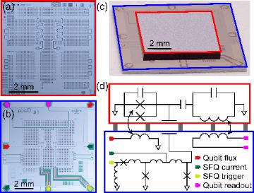
SEEQC SFQ-controlled 5-qubit system
SEEQC SFQ-controlled 5-qubit system
Register profile — the machine's variant of its architecture
qubit type: transmon
gate mechanism: no entangling gate published under SFQ control; single-qubit charge control by SFQ digital pulse trains
connectivity: not published
control: Single Flux Quantum digital logic co-located with the qubits at 10 mK; integrated digital demultiplexing so several qubits share one control pathway; ~1 nW per qubit
control placement: SFQ at mK
readout: dispersive
gate evidence: no published figure
flags: 1q only
Technologies by layer — the machine's cell per layer
| 1 Qubit carrier | |
| 2 Encoding | Bare physical qubit (no encoding) · primary ◌ 🔎 Bare two-level subspace — Computational subspace of an anharmonic oscillator; leakage to |2⟩ is the price. |
| 3 Gate mechanism | — undisclosed — exists, nothing published ▣ Fig. S2 (2Q Gate Results); Supp. §I 2Q Calibration and Benchmarking ✅ no entangling gate published under SFQ control; single-qubit charge control by SFQ pulse trains, 1Q >99.5%, peaks >99.9% (Mar 2026) |
| 4 Connectivity / transport | Static nearest-neighbour lattice · primary ▤ Supp. §A Device Design and Fabrication (centre qubit capacitively coupled to 4 outer qubits); Fig. S1 (Experimental Diagram) ✅ connectivity not published; 5-qubit system |
| 5 Control | SFQ digital control (4 K / mK) · primary ▣ Fig. 1 (RT vs 4K cryo-CMOS vs integrated SFQ control); Fig. 3 (SFQ demultiplexer); Fig. S3 (SFQ Circuit Schematics); §Demultiplexer (DMX) Results; §Power Dissipation ✅ SFQ digital logic co-located with qubits at 10 mK; digital demultiplexing, <1 line per qubit; ~1 nW per qubit; no detectable quasiparticle poisoning (Mar 2026) |
| 6 Readout | Dispersive microwave readout (+TWPA, Purcell) · primary ▤ Supp. §B Experimental Setup; Fig. S1 (Experimental Diagram) 🔎 dispersive; digital on-die readout is a stated next milestone |
| 7 Code | |
| 8 Decoder | |
| 9 Interconnect | Multi-die packaging in one module (flip-chip, bump-bonded control die) · primary ▤ Supp. §A Device Design and Fabrication ✅ flip-chip: 5×5 mm quantum chip bump-bonded (indium on an Al hard stop, 10 µm gap) to a 10×10 mm carrier chip with all passive wiring and SFQ elements; signals couple across the vacuum gap |
| 10 Manufacturing | Superconducting-qubit lithography (Al/AlOx/Al junctions, Nb wiring, 300 mm) · primary ▤ Supp. §A Device Design and Fabrication (SEEQC SFQuClass Nb process, 1 kA/cm2 JJs, high-kinetic-inductance layer) ✅ |
Standard records
control lines per qubit → 1 lines/qubit · best (digital demultiplexing at mK; exact ratio not published)
power ~1e-9 W per qubit at mK · Mar 2026 · source
evidence: ✅ 6 / 10
Pictures
Every picture carries the story of what it shows and its credit line.