Advantage
Advantage
Register profile — the machine's variant of its architecture
qubit type: rf-SQUID flux qubit (analog Hamiltonian carrier)
gate mechanism: analog annealing evolution; not a gate
connectivity: Pegasus, degree 15
control: on-chip flux DACs + superconducting control circuitry
control placement: on-chip flux DAC
readout: QFP / SQUID flux readout through on-chip shift registers
gate evidence: no published figure
codes: qac
flags: annealer reference only
Technologies by layer — the machine's cell per layer
| 1 Qubit carrier | rf-SQUID flux qubit (annealer) · primary ▤ §Experimental testbed (ADV1: 5,627 qubits, Pegasus, cryostat set point 12 mK) ✅ rf-SQUID flux qubit (analog Hamiltonian carrier); 5,000+ qubits; DEPLOYED Sep 2020, still in service |
| 2 Encoding | — none — nothing in this layer ◌ 🔎 analog annealer has no encoding layer; the anneal architecture declares an empty L2 |
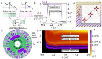
| 3 Gate mechanism | Quantum annealing (analogue evolution) · primary ▣ §Quantum annealing (Methods); Fig. 5 (dynamical scaling, ta = 7 ns and 20 ns quenches) ✅ analog annealing evolution; not a gate |
| 4 Connectivity / transport | Long-range on-chip couplers (c-couplers, mm-scale) · primary ▣ Fig. 1 (roadway drawing of Pegasus P3: internal/external/odd couplers); §2 Pegasus family of topologies ✅ Pegasus topology, degree 15 |
| 5 Control | On-chip flux-DAC multiplexing · primary ▣ Fig. 3–5 (Φ-DAC schematic, SFQ sources); Fig. 8 (XYZ addressing); §III Design and operation of a Φ-DAC ✅ on-chip flux DACs + superconducting control circuitry |
| 6 Readout | Flux readout via QFP / SQUID shift registers (annealers) · primary ▤ §readout (QFP shift register; microresonator frequency multiplexing) ✅ QFP-based shift registers move qubit states along horizontal and vertical tracks to edge microresonators read in parallel by frequency multiplexing; Advantage_system4 readout 17–235 µs, error ≤ 0.001 (solver properties) Dispersive microwave readout (+TWPA, Purcell) · alternate ◌ 🔎 path-assigned ro_disp describes transmon readout, not annealer readout; actual is QFP/SQUID flux readout |
| 7 Code | — (Atlas gap: ∅G-qac) · primary ▤ abstract ✅ quantum annealing correction (penalty-repetition encoding) on up to 1,322 logical qubits of Advantage 4.1 (sweep 7 Oct 2026, source read) |
| 8 Decoder | |
| 9 Interconnect | — none — nothing in this layer ◌ 🔎 monolithic single QPU, no interconnect; no machine-specific source |
| 10 Manufacturing | Superconducting-qubit lithography (Al/AlOx/Al junctions, Nb wiring, 300 mm) · primary ▣ §III.D Minimizing Φ-DAC footprint (6 Nb metal layers, 250 A/cm² trilayer); Fig. 9 (chip micrograph) ✅ superconducting flux-qubit lithography (in-house D-Wave process not published); no machine-specific fab source |
Standard records
connectivity degree → 15 neighbours · typical (Pegasus)
Sep 2020 · source
evidence: ✅ 7 / 11
Pictures
Every picture carries the story of what it shows and its credit line.