Single-photon detection (SNSPD / TES) ro_spd
Cryogenic superconducting detectors that destroy a photon to register it; the shared readout organ of every photonic and photon-linked platform.
Single-photon detection (SNSPD / TES)
Destructive by nature; 93.4% wafer-scale median to 99.73% on a hero device, 3 ps jitter, 1–4 K; thousands of channels needed.
Brief →Key references
Design space — attributes
- (a) carrier affinity
- photon (natural particle, engineered modes)
- (b) time · entangling
- —
- (c) readout
- single-photon detection · 10 ns · destructive · no mid-circuit
- (d) mobility
- —
- (e) control
- electro-optic @ 4 K stage
- (f) error structure
- loss (erasure)
- (g) manufacturing
- photonic IC foundry
Evaluation space — dated attributes
The '98.9% median (PsiQuantum)' sometimes quoted is superseded: the Omega paper gives 93.4% median on-chip efficiency — 0.30 dB per detection rather than 0.05 dB.
Standard records
Actors & goals — annotations
Edges
Used by 14 machines (13 primary · 1 alternate)
- photonics 14
- ETRI 8-photon silicon-photonic qubit chip ETRI (with KAIST and the University of Trento) paper ▨ ✅
- PT-1 ORCA Computing paper product page ▤ §2.2 Physical devices ('only a single photon detection device') ✅
- PT-2 ORCA Computing product page press ▤ §2.2 Physical devices ✅
- Omega chipset (Moreton Bay / Chicago systems unnamed) PsiQuantum paper product page press ▣ Fig. 2e (SNSPD efficiency); Fig. 4d–f (PNRD) ✅
- Belenos Quandela product page press ▤ Methods: Architecture (12 SNSPD outputs + time-to-digital converter) ✅
- Quandela Canopus Quandela product page product page press ◌ 🔎
- Lucy Quandela press ▦ 🔎
- Carina QuiX Quantum ▨ 🔎
- Jiuzhang (1.0) USTC (Pan Jianwei group) press ▤ Abstract ✅
- Jiuzhang 2.0 USTC (Pan Jianwei group) paper press ▤ 🔎
- Jiuzhang 3.0 USTC (Pan Jianwei group) paper press ▤ Abstract ✅
- Jiuzhang 4.0 USTC (Pan Jianwei group) paper press ▣ Fig. 1 (experimental setup, 16 detection channels) ✅
- Borealis Xanadu paper link ▤ Methods: Optical circuit (demux, TES) ✅
- Aurora Xanadu paper press link ▣ Fig. 2 (cryogenic PNR array); Methods: PNR detection system ✅ (alternate)
Pictures
Every picture carries the story of what it shows and its credit line.
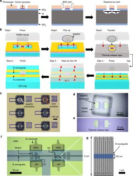

Single-photon detection (SNSPD / TES)
Cryogenic superconducting detectors that destroy a photon to register it; the shared readout organ of every photonic and photon-linked platform.
Verdict. Efficiency is solved in the lab (99.73% on-chip) but not at wafer scale (93.4% median on Omega); channel count and cryogenics, not physics, decide whether photonic fault tolerance is buildable.
Λ = error-suppression factor per code-distance step; QBI = DARPA Quantum Benchmarking Initiative (Stage A concept → B R&D plan → C government V&V); G1–G7 = the report's goal classes (see Actors & economics).
Identity & lineage
A current-biased superconducting nanowire absorbs one photon, forms a resistive hotspot and emits a voltage pulse; a transition-edge sensor (TES) instead measures the absorbed energy calorimetrically and so resolves photon number. Gol'tsman's group at Moscow State Pedagogical University demonstrated the first NbN device in 2001 D[626]; the voltage-biased TES dates to Irwin (1995) D[627]. Scontel, still in Moscow, descends directly from that first group.
Attributes. Carrier affinity: fabricated — a lithographic thin film, not a natural quantum system. Characteristic time and entanglement: not applicable; the node hosts no qubit and performs no entangling operation. Readout: single-photon detection, ~1.0×10⁻⁸ s per event including reset, destructive, not mid-circuit — the photon is consumed. Mobility: none; a fixed terminal. Control modality and placement: electro-optical bias and amplification at the 1–4 K stage. Dominant error structure as the code sees it: loss — a missed detection is an erasure at a known location, a dark count a false positive the decoder cannot distinguish from a real click. Manufacturing: photonic-integrated-circuit process, increasingly the one that carries the waveguides.
Physics & limits
A 1550 nm photon carries 0.80 eV against an NbN gap of a few meV, so absorption breaks of order 10³ Cooper pairs; the signal is enormous relative to the gap, which is why internal detection efficiency saturates near unity (99.99% at 5.5 µA bias D[628]). Efficiency is therefore an optics problem, not a superconductivity problem: it factorises into fibre coupling × absorption × internal efficiency, and the art is removing the first term (waveguide integration) or engineering the second (dielectric mirrors D[618]). The real floors are timing and rate: reset is kinetic inductance over load, about 10 ns, capping per-pixel rates in the tens of Mcps, while jitter has a Fano floor from hotspot statistics plus a geometric term along the wire — which is why 2.7 ± 0.2 ps FWHM at 400 nm degrades to 4.6 ± 0.2 ps at 1550 nm D[629]. TES trades both away: number resolution for ~µs recovery at ~100 mK, a dilution refrigerator rather than a 2–4 K cold head.
In the currency photonic fault tolerance uses, 1% inefficiency costs 0.044 dB. PsiQuantum's 93.4% median on-chip efficiency D[169] costs 0.30 dB against a fusion per-photon budget near 0.5 dB, and its 6.6% inefficiency alone is 2.4× the 2.7% loss threshold of 6-ring fusion schemes S[179]. Nothing else here matters as much as that arithmetic.
Engineering state of the art
Best demonstrated is a cascaded waveguide pair at 99.73% on-chip efficiency, 1.5 K, NbN, 100 nm wide and 5 nm thick D[628]. Typical at scale is different: 93.4% median on-chip across PsiQuantum's 300 mm Omega wafers at ~2 K D[169], and catalogue systems quoting only ">90% near 1550 nm" with sub-100 ps jitter C[630], [631]. The gap between a hero device and a wafer median is the engineering problem. The dominant term today is inefficiency convolved with waveguide and switch loss; in a networking machine it is dark counts and jitter against the coincidence window.
table
| Year | Figure | Who | Tag+key |
|---|---|---|---|
| 2001 | First NbN nanowire single-photon detector | Moscow State Pedagogical University | D[626] |
| 2008 | TES 95% efficiency at 1556 nm, photon-number resolving | NIST Boulder | D[632] |
| 2020-11 | System detection efficiency 98.0 ± 0.5% at 1550 nm, fibre-coupled | NIST | D[618] |
| 2020 | Timing jitter 2.7 ± 0.2 ps FWHM at 400 nm; 4.6 ± 0.2 ps at 1550 nm | JPL | D[629] |
| 2023-10 | 400,000-pixel camera, 4 × 2.5 mm, thermal row–column readout | NIST Boulder | D[339] |
| 2025-02 | Median on-chip efficiency 93.4% at ~2 K, 300 mm foundry line | PsiQuantum | D[169] |
| 2025-10 | On-chip efficiency 99.73% cascaded (97.33% single), 1.5 K | Nanjing University | D[628] |
Manufacturing, materials & supply chain
Four material systems compete: NbN and NbTiN (fast, 2–4 K, the commercial default), amorphous WSi (highest efficiency, ~1 K, NIST's choice for records) and MoSi. Amorphous films are more uniform across a wafer, which is what a 300 mm line needs; polycrystalline NbN is faster. PsiQuantum's integration of detectors into a GlobalFoundries 300 mm flow alongside SiN waveguides and barium-titanate switches is the only wafer-scale datapoint, and its published median — not its best die — is the honest yield statement D[169].
The supply chain is short and concentrated. Merchant vendors are Single Quantum (Delft), ID Quantique (Geneva, IonQ-owned since 2025), Photon Spot (Monrovia, CA), Quantum Opus (Michigan) and Scontel (Moscow); NIST and JPL set the records but sell nothing. Every one ships inside a closed-cycle cryostat, so the single point of failure is upstream: Gifford-McMahon and pulse-tube cold heads from a handful of makers (Sumitomo Heavy Industries, Cryomech, and integrators such as Bluefors), plus helium-4, cryogenic coax and fibre feedthroughs. Photon Spot mitigates this by selling its own Cryospot cryostats C[630].
Export-control exposure sits on the cryogenics, not the detector. The BIS interim final rule of 2024-09-06 created ECCN 3A904 for cryogenic refrigeration below 4.5 K, with 3A901.b for quantum-limited amplifiers fact[301]; single-photon detectors are not named, but the box they live in is controlled. Scontel's Moscow location makes it effectively unavailable to Western programmes post-2022 — a judgment, not a sourced fact.
Control, readout & I/O burden
Per channel: a bias current, an amplifier, a coaxial line from 1–4 K to room temperature, and a time-tagger input. Tolerable at 10¹–10² channels — the entire commercial market — and binding above it. At 10³ the coax heat load and 2–4 K cooling budget dominate; Bluefors' KIDE, with nine pulse-tube cryocoolers and "more than 4,000 RF lines" Cfact[303], is roughly the shippable ceiling. At 10⁴ wiring must give way to multiplexing: the 400,000-pixel camera's thermal row–column scheme D[339] shows this works when timing can be sacrificed, but fusion networks need MHz–GHz feed-forward from click to switch and cannot sacrifice it. At 10⁶ detector, amplifier and demultiplexer must be monolithic in the photonic process and the cryoplant becomes kilowatt-class at 2–4 K; PsiQuantum's DARPA Stage C work explicitly covers packaging and cryogenics validation Pfact[181], and the Linde cryoplant for its Moreton Bay site is not due for delivery until 2H 2027 Cfact.
Role in the stack
The node sits on the fusion-based discrete-variable architecture (PsiQuantum, Quandela, QuiX), the continuous-variable/GKP architecture (Xanadu) and the boson sampler. It requires single photons and provides heralding for linear-optical fusion plus photon detection for the ion–photon and spin–photon interconnects: one part is the readout organ for three otherwise unrelated modalities. Derived clock = sum of the syndrome round: gate layers + transport + readout + reset — no such round on a photonic architecture; the detector contributes ~1.0×10⁻⁸ s, so it is never the slow term for ion or defect links (rates 10–250 s⁻¹ D[115], [116]) and only marginally so for fusion, where feed-forward latency dominates.
It conflicts with the surface code specifically: destructive detection precludes repeated syndrome extraction on the same photon, so photonic QEC must regenerate carriers between rounds. Switching away is asymmetric — Xanadu's CV architecture uses room-temperature homodyne for most measurements and needs number resolution only for GKP preparation D[173], [174]. Neighbouring empty slots: a room-temperature >99% number-resolving detector, and any non-destructive telecom photon counter, which would dissolve the conflict above.
Evidence — how the numbers were measured
System detection efficiency is measured against a heavily attenuated laser and a calibrated power meter whose uncertainty the Nanjing authors put at 2–5% D[628] — comparable to the gap between the 98.0 ± 0.5% D[618] and 99.73% D[628] headlines. The two are also different quantities: on-chip efficiency excludes fibre-to-chip coupling, so waveguide-integrated records must never be tabulated beside fibre-coupled ones without that caveat. Uncaptured: afterpulsing, latching, blinding attacks, and the joint distribution of efficiency and jitter across a wafer, which is what an integrator needs.
Conflict. A "98.9% median (PsiQuantum)" figure is quoted elsewhere; the Omega paper and the shared fact record both give 93.4% median on-chip D[169]fact. The primary-source figure, 93.4%, stands; the difference is 0.30 dB versus 0.05 dB per detection.
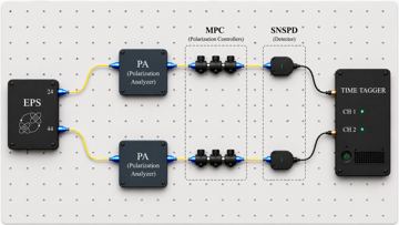
Silicon avalanche photodiodes, still used instead of superconducting nanowire or transition-edge detectors to characterise sources, emit breakdown flashes that leak between the two detectors of a Hanbury Brown–Twiss set-up (a beam splitter feeding two detectors whose coincidences measure the multiphoton fraction) and raise the zero-delay coincidence peak in the near-infrared; a second-order correlation g⁽²⁾(0) measured this way is an upper bound on the multiphoton fraction P[887].
Cold-head supplier concentration (Sumitomo Heavy Industries, Cryomech) and Scontel's unavailability to Western programmes after 2022 are analyst judgments, not sourced facts. The abstract of Korzh et al. gives the jitter figures but not that device's operating temperature or detection efficiency. Not published: the ID Quantique acquisition consideration, and SNSPD system prices or vendor revenues from Single Quantum, Photon Spot, Quantum Opus or Scontel, so unit economics cannot be checked.
Actors & economics
Who.
| Organisation | Role | Country | What exactly they do | Evidence |
|---|---|---|---|---|
| PsiQuantum | developer | US | In-house SNSPDs monolithic in Omega on 300 mm GlobalFoundries, 93.4% median | D[169] |
| Single Quantum | supplier | NL | Turnkey SNSPD systems; 400th shipped to Q*Bird 2026-07 | P[621] |
| ID Quantique | supplier | CH | SNSPD and InGaAs detectors plus QKD; IonQ-acquired 2025-05-06 | P[633] |
| Photon Spot | supplier | US | SNSPDs plus its own Cryospot cryostats; >90% QE, sub-100 ps jitter | C[630] |
| Quantum Opus | supplier | US | Opus One, ≥90% at 1310/1550 nm, >2 K, number-resolving under licence | C[631] |
| Scontel | supplier | RU | Large-area, ultra-low-noise and number-resolving SSPD lines | C[634] |
| NIST Boulder | research | US | 98.0% efficiency record, WSi films, 400 kpixel camera, calibration | D[339], [618] |
| JPL | research | US | 2.7 ps jitter record; deep-space optical-comms arrays | D[629] |
| Nanjing University | research | CN | 99.73% cascaded on-chip efficiency | D[628] |
| Xanadu | user | CA | CV architecture leans on homodyne; number resolution only for GKP | D[173] |
| Bluefors | supplier | FI | Cryogenic platforms; KIDE, nine pulse-tube coolers, >4,000 RF lines | C[303] |
Money.
- 2025-05-06 · IonQ / ID Quantique · M&A · consideration not disclosed in the cited releases · — · closed P[633]
- 2025-09-10 · PsiQuantum · Series E · $1 B at $7 B · BlackRock, Temasek, Baillie Gifford · closed fact
- 2025-11-06 · DARPA QBI Stage B · programme · up to $15 M each, 11 performers incl. Xanadu, Photonic Inc. · DARPA · awarded fact[65]
- 2026-03-26 · Xanadu · SPAC close · ~$302 M gross, ~40% below plan · Crane Harbor · closed fact
- 2026-05-21 · PsiQuantum · CHIPS letter of intent · $100 M · US Dept of Commerce · LOI (non-binding) fact[300]
- 2026-06-16 · Quandela · DARPA QBIT Stage A · amount not disclosed · DARPA · announced fact
- 2026-07-04 · Single Quantum · 400th SNSPD system delivered · revenue not disclosed · Q*Bird · reported P[621]
- 2026-07-22 · PsiQuantum · DARPA QBI Stage C expansion (switches, packaging, cryogenics V&V) · $125 M, after $31.8 M in 2025-09 · DARPA · announced Pfact[181]
- 2026-08-28 · Xanadu · Canadian factory funding · CAD 195 M · federal programme · announced C[178]
No detector vendor appears in that ledger with a disclosed round: the merchant supply base is private, opaque, and an order of magnitude smaller than the platform vendors depending on it.
Market & supply chain. No vendor publishes prices C[630], [631], [634], so unit economics are unverifiable. Paying demand today is G6 networking — QKD, where Single Quantum's 400 systems and ID Quantique's line live — plus a non-quantum anchor in G7 deployable systems (deep-space and lunar optical communications; NASA, NIST, Fermilab, Sandia and Argonne are named customers C[630], [631]). G3/G4 pays only through PsiQuantum, Xanadu, Quandela, QuiX and Photonic Inc. Concentration risk is upstream: cold heads, helium, cryogenic coax.
IP & standards. Quantum Opus holds an exclusive licence to US 11,274,962 B2 for photon-number resolution C[631]. No dated patent-count figure from a named database was found for this node as of 2026-09-03. There is no SNSPD-specific standard; calibration traceability is de facto NIST's D[339], [618].
Roadmaps & track record. PsiQuantum (promised since 2021 · useful system by end-2027 · at risk: Moreton Bay groundbreaking only 2026-06, cryoplant delivery due 2H 2027 Cfact, no 2026 hardware demonstration published) P[181]. Xanadu (promised 2026-08-31 · loss 24.1× above threshold in 2026 → 1.0× in 2030, 1,000+ logical qubits by 2031 · paper roadmap only) C[178]. Single Quantum (no public roadmap; 400 delivered systems is the only dated metric) P[621]. Credibility: the detector vendors under-promise and ship; PsiQuantum's detector physics is credible and its schedule is not; Xanadu's roadmap is three weeks old and untested.
Strategic reading. If fusion-based photonic computing scales, detectors per machine go from 10² to 10⁶ and merchant vendors must become foundry-integrated IP licensors or be displaced by in-house monolithic detectors — PsiQuantum has already chosen the second outcome for itself. Supplier bargaining power is weak against platform vendors and strong only in QKD and space communications, where volumes are real and integration is not. The substitution threat is homodyne detection on the CV architecture: cheap and room-temperature. The quiet winner in every scenario is the cryocooler industry.
Outlook & open questions
Confirm in 12–24 months if a published wafer map shows >99% median on-chip efficiency across a 300 mm line; if a >10³-channel cryogenic readout is demonstrated with per-channel jitter and feed-forward latency; if PsiQuantum's Moreton Bay cryoplant is delivered in 2H 2027 as promised Cfact. Demote if PsiQuantum publishes no detector data through 2027, or wafer medians stay below 95% while switch and coupling losses fall. Best case by 2029: waveguide-integrated detectors above 99% median with thousands of channels multiplexed on chip. Worst case: records keep being set on two-detector laboratory devices while wafer medians stall near 93–95% and the 2.7% loss threshold stays unreachable.
Open questions. (1) What is the efficiency–jitter joint distribution across a 300 mm wafer, and what is the yield criterion? (2) Can number resolution be had at 2 K, or does GKP permanently require a TES near 100 mK? (3) What cooling power per channel at 2 K does a 10⁵-channel machine need, and who builds that plant? (4) Does any non-destructive scheme reach telecom wavelengths with usable efficiency? (5) Do merchant vendors have a foundry-compatible path? Watch PsiQuantum's next hardware paper and Stage C milestones, and any disclosed round at Single Quantum, Photon Spot or Quantum Opus — the first signal that demand has moved beyond QKD.
References
- [65] DARPA, “Stage B selection,” Nov. 6, 2025. [Online]. Available: https://www.darpa.mil/
research/ Gprograms/ quantum-benchmarking-initiative/ stage-b-selection - [115] D. Main et al., “Distributed quantum computing across an optical network link,” Nature, vol. 638, no. 8050, pp. 383–388, Feb. 2025, doi: 10.1038/s41586-024-08404-x. D
- [116] J. O'Reilly et al., “Fast photon-mediated entanglement of continuously-cooled trapped ions for quantum networking,” Phys. Rev. Lett., vol. 133, Art. no. 090802, Aug. 2024, doi: 10.1103/PhysRevLett.133.090802. arXiv:2404.16167. D
- [169] K. Alexander et al., “A manufacturable platform for photonic quantum computing,” Nature, vol. 641, no. 8064, pp. 876–883, Feb. 2025, doi: 10.1038/s41586-025-08820-7. D
- [173] H. A. Rad et al., “Scaling and networking a modular photonic quantum computer,” Nature, vol. 638, no. 8052, pp. 912–919, Jan. 2025, doi: 10.1038/s41586-024-08406-9. D
- [174] M. V. Larsen et al., “Integrated photonic source of Gottesman–Kitaev–Preskill qubits,” Nature, vol. 642, no. 8068, pp. 587–591, Jun. 2025, doi: 10.1038/s41586-025-09044-5. D
- [178] Xanadu Quantum Technologies Limited, “Xanadu Charts Path to Over 1,000 Logical Qubits by 2031,” GlobeNewswire, Aug. 31, 2026. [Online]. Available: https://www.globenewswire.com/
news-release/ C2026/ 08/ 31/ 3353211/ 0/ en/ xanadu-charts-path-to-over-1-000-logical-qubits-by-2031.html - [179] S. Bartolucci et al., “Fusion-based quantum computation,” Nat. Commun., vol. 14, Art. no. 912, Feb. 2023, doi: 10.1038/s41467-023-36493-1. arXiv:2101.09310. S
- [181] M. Abdel-Kareem, “PsiQuantum Secures $125 Million Expanded Agreement with DARPA under QBI Program,” Quantum Computing Report, Jul. 22, 2026. [Online]. Available: https://quantumcomputingreport.com/
psiquantum-secures-125-million-expanded-agreement-with-darpa-under-qbi-program/ P - [300] National Institute of Standards and Technology, “Department of Commerce Announces Letters of Intent With 9 Companies for $2 Billion to Accelerate U.S. Leadership in Quantum Computing,” NIST News, May 21, 2026. [Online]. Available: https://www.nist.gov/
news-events/ Gnews/ 2026/ 05/ department-commerce-announces-letters-intent-9-companies-2-billion - [301] US Department of Commerce, Bureau of Industry and Security, “Commerce Control List Additions and Revisions; Implementation of Controls on Advanced Technologies Consistent With Controls Implemented by International Partners,” Federal Register, vol. 89, p. 72926, Sep. 6, 2024. [Online]. Available: https://www.federalregister.gov/
documents/ G2024/ 09/ 06/ 2024-19633/ commerce-control-list-additions-and-revisions-implementation-of-controls-on-advanced-technologies - [303] Bluefors, “KIDE Cryogenic Platform — For Large-Scale Quantum Computing,” Jun. 16, 2026. [Online]. Available: https://bluefors.com/
products/ Ckide-cryogenic-platform/ - [339] B. G. Oripov et al., “A superconducting nanowire single-photon camera with 400,000 pixels,” Nature, vol. 622, no. 7984, pp. 730–734, Oct. 2023, doi: 10.1038/s41586-023-06550-2. D
- [618] D. V. Reddy, R. R. Nerem, S. W. Nam, R. P. Mirin, and V. B. Verma, “Superconducting nanowire single-photon detectors with 98% system detection efficiency at 1550 nm,” Optica, vol. 7, no. 12, p. 1649, Dec. 2020, doi: 10.1364/OPTICA.400751. D
- [621] TipRanks, “Single Quantum Hits 400-System Milestone as It Deepens European Quantum Partnerships,” Jul. 4, 2026. [Online]. Available: https://www.tipranks.com/
news/ Pprivate-companies/ single-quantum-hits-400-system-milestone-as-it-deepens-european-quantum-partnerships - [626] G. N. Gol'tsman et al., “Picosecond superconducting single-photon optical detector,” Appl. Phys. Lett., vol. 79, no. 6, pp. 705–707, Aug. 2001, doi: 10.1063/1.1388868. D
- [627] K. D. Irwin, “An application of electrothermal feedback for high resolution cryogenic particle detection,” Appl. Phys. Lett., vol. 66, no. 15, pp. 1998–2000, Apr. 1995, doi: 10.1063/1.113674. D
- [628] Z.-G. Li et al., “Surpassing 99% detection efficiency by cascading two superconducting nanowires on one waveguide with self-calibration,” Light: Science & Applications, vol. 14, no. 1, Art. no. 369, Oct. 2025, doi: 10.1038/s41377-025-02031-5. D
- [629] B. A. Korzh et al., “Demonstration of sub-3 ps temporal resolution with a superconducting nanowire single-photon detector,” Nat. Photon., vol. 14, no. 4, pp. 250–255, Mar. 2020, doi: 10.1038/s41566-020-0589-x. arXiv:1804.06839. D
- [630] Photon Spot, “Photon Spot — Cryogenic & Quantum Detection Systems.” [Online]. Available: https://www.photonspot.com/ C
- [631] Quantum Opus, “World-Class Photon Detection. Simplified.” [Online]. Available: https://www.quantumopus.com/ C
- [632] A. E. Lita, A. J. Miller, and S. W. Nam, “Counting near-infrared single-photons with 95% efficiency,” Optics Express, vol. 16, no. 5, Art. no. 3032, 2008, doi: 10.1364/OE.16.003032. D
- [633] IonQ, “IonQ Completes Acquisition of ID Quantique, Cementing Leadership in Quantum Networking and Secure Communications,” May 6, 2025. [Online]. Available: https://investors.ionq.com/
news/ Pnews-details/ 2025/ IonQ-Completes-Acquisition-of-ID-Quantique-Cementing-Leadership-in-Quantum-Networking-and-Secure-Communications/ default.aspx - [634] SCONTEL, “SCONTEL: SSPD SNSPD HEB CRYOGENICS – DETECT EVERYTHING YOU WANT.” [Online]. Available: https://www.scontel.ru/ C
- [887] S. Luo et al., “100 million photons per second from a single organic molecule,” arXiv:2609.29736, Sep. 2026. P