Spin–photon solid-state link (SiV, NV, T centre) ic_spinphoton
Heralded photonic entanglement between separated solid-state spin registers — diamond NV and SiV centres, silicon T centres — through deployed telecom fibre.
Spin–photon solid-state link (SiV, NV, T centre)
Entanglement over 25–35 km deployed fibre at 0.02–1 Hz with F 0.53–0.86; two distinct inter-cryostat teleported-CNOT results — post-selected on T centres (Photonic Inc.) and unconditional on NV (QuTech).
Key references
Design space — attributes
- (a) carrier affinity
- intermediate / carrier-agnostic
- (b) time · entangling
- —
- (c) readout
- —
- (d) mobility
- flying qubits (photons)
- (e) control
- optical @ room temperature
- (f) error structure
- loss (erasure)
- (g) manufacturing
- diamond growth / implantation
Evaluation space — dated attributes
Both results exist and differ in kind: Photonic Inc.'s 2024 T-centre demonstration is a post-selected preprint with a truth table rather than a gate fidelity; QuTech's 2026 NV result is unconditional. Quoting them together without that distinction overstates the T-centre platform.
Actors & goals — annotations
Edges
Used by 1 machine (1 primary · 0 alternate)
- defect spins 1
- Entanglement First modules Photonic Inc. paper product page product page ▨ ✅
Pictures
Every picture carries the story of what it shows and its credit line.
Spin–photon solid-state link (SiV, NV, T centre)
Heralded photonic entanglement between separated solid-state spin registers — diamond NV and SiV centres, silicon T centres — through deployed telecom fibre.
Verdict. Inter-cryostat gates exist on both hosts, unconditionally on NV (63–64%) and only post-selected on T centres. Rates of 0.0075–1 Hz sit 10⁵–10⁷ below the ~200 kHz reported as Photonic Inc.'s architecture target, an unverified figure; loss, not coherence, is why.
Λ = error-suppression factor per code-distance step; QBI = DARPA Quantum Benchmarking Initiative (Stage A concept → B R&D plan → C government V&V); G1–G7 = the report's goal classes (see Actors & economics).
Identity & lineage
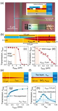
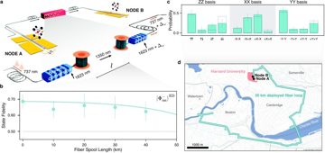
Each node is a spin qubit in a solid — a nitrogen-vacancy or silicon-vacancy centre in diamond, or a silicon T centre — whose optical transition emits a photon entangled with the spin. Photons from two nodes interfere on a beamsplitter; a detection pattern heralds spin–spin entanglement without trusting the channel, so loss costs attempts, not fidelity. Delft demonstrated the first heralded solid-state version across 3 m in 2013 D[783]; everything since has pushed that protocol into deployed telecom fibre.
- Mobility: the carrier flies (a photon in fibre); both spins stay fixed.
- Error structure: loss-dominated; conditional fidelity and unconditional rate must be quoted together.
Physics & limits
The floor is the product of collection, conversion and transmission efficiencies, entering the rate quadratically for two-photon protocols and linearly for the single-photon protocol Delft uses at metropolitan scale D[784]. The coherent zero-phonon line carries ~3% of an NV centre's emission, ~23% of a T centre's and 65–90% of an SiV's Dfact, and a 35 km deployed urban loop costs a further 17 dB D[209]. Wavelength decides whether conversion is needed — NV at 637 nm and SiV at 737.2 nm require it (Harvard converts to 1,350 nm), while a T centre emits natively near 1,326 nm, skipping that stage but paying with a weaker transition P[363]. Spin coherence is not the constraint: nuclear memories hold entanglement beyond 2 s D[209], far longer than the 0.25–0.35 ms fibre round trip. The one lever that moves the floor is cavity enhancement — a fibre microcavity around one NV raised resonant collection roughly tenfold, ~0.05% to ~0.5%, keeping echo coherence above 100 µs D[359]; one more such step would pass the ~2% per-attempt photon success that 0.8-NA objectives give a trapped ion D[116].
Engineering state of the art
table
| Year | Figure | Who | Tag+key |
|---|---|---|---|
| 2024-04 | NV, nodes 10 km apart over 25 km deployed fibre with telecom L-band conversion: F = 0.534 at 0.022 s⁻¹ | QuTech/Delft | D[784] |
| 2024-05 | SiV: F = 0.69(7) between nuclear memories over a 35 km deployed Boston loop; 0.86(3) electron–electron at 20 m, ≤1 Hz | Harvard | D[209] |
| 2024-06 | T centre, two modules in separate cryostats over ~40 m fibre: Bell F = 0.60(8), ~7.5 mHz; teleported-CNOT sequence post-selected, no gate fidelity | Photonic Inc. | P[363] |
| 2026-05 | Unconditional teleported CNOT between NV registers in separate cryostats: 4-qubit GHZ 64(4)%, CNOT-mediated state 63(4)% | QuTech/Delft | Dfact |
The dominant term is collection and heralding efficiency, not spin coherence or in-node gate error.
Manufacturing, materials & supply chain
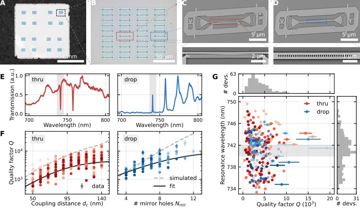
Diamond nodes need quantum-grade CVD material, for which Element Six (UK) is the reference supplier Pfact, plus nanophotonic cavities whose yield is the blocker and is unpublished: a 2026 Delft tin-vacancy study characterised 327 cavities on two chips at room temperature, found coupled centres in 7 of the 9 it cooled and measured two above cooperativity one Dfact — no chip-wide fraction, the number any 10²-node proposal needs. Silicon T centres trade emitter quality for process maturity: implantation into enriched ²⁸Si on a CMOS line, with the centres operated at ~1.5–4 K, not millikelvin P[785]. Both ends depend on nanowire detectors from a five-vendor merchant base — Single Quantum, ID Quantique (owned by IonQ), Photon Spot, Quantum Opus and Moscow's Scontel Pfact. No export-control classification names spin–photon links.
Control, readout & I/O burden
Per node: a cryostat, microwave spin control, resonant lasers for initialisation and readout, a conversion stage unless the emitter is already telecom, phase-stabilised fibre to the midpoint, and detectors. The binding burden is duty cycle, not latency: at 0.022 s⁻¹ one link spends 45 s per Bell pair while stabilisation loops run continuously. Ten nodes are an experiment; 10² at sub-Hz cannot serve a distributed processor, and 10³ needs multiplexed emitters and detector arrays nobody has fielded.
Role in the stack
It requires a colour-centre spin register and single-photon detection; without low-dark-count detectors heralding fails outright. It provides for nothing further and tops the defect-spin network architecture. On any distributed architecture it is the pacing term: no code runs on the defect architecture, so in place of a sum of the syndrome round: gate layers + transport + readout + reset the clock is 45 s at Delft's metropolitan rate and 1.0 s at Harvard's best. The comparison that matters is the competing interconnect: Oxford's trapped-ion link reached 96.89(8)% Bell fidelity at 9.7 s⁻¹ with an 86.2(9)% teleported CZ Dfact — against Harvard's best SiV link, 0.86(3) at up to 1 Hz over 20 m, about ten times the rate and 11 points higher, and its teleported gate 23 points above QuTech's unconditional 63(4)% D[209]Dfact. Solid-state's counter-argument is manufacturability, not performance.
Evidence — how the numbers were measured
The teleported-CNOT attribution resolves, and not as a mis-attribution: both results exist and differ in kind. Photonic Inc. entangled two T-centre modules in separate cryostats over ~40 m and ran a teleported-CNOT sequence, but forwent feed-forward and post-selected on a photon detection, reporting a truth table rather than a gate fidelity; still a 2024 preprint as of 4 Sep 2026 P[363]. QuTech's 2026 result is unconditional — real-time feed-forward, no post-selection — at 63(4)% and 64(4)% Dfact. Quoting the two together without that distinction overstates the T-centre platform. Elsewhere fidelities are conditional on a herald, and Harvard rejects ~23% of data on reflectance-contrast thresholds D[209]. No result here has a second-group replication.
Not published: a dated patent-family count for spin–photon links.
Actors & economics
Who.
| Organisation | Role | Country | What exactly they do | Evidence |
|---|---|---|---|---|
| QuTech | Research | Netherlands | Metropolitan NV link; the only unconditional inter-cryostat gate | Dfact |
| Photonic Inc. | Developer | Canada | Silicon T-centre modules, native telecom emission | P[363] |
| Harvard University | Research | USA | SiV nanophotonic nodes over a 35 km deployed loop | D[209] |
| Fujitsu | Funder | Japan | Funds the Delft modular-computer joint programme | Pfact |
| Microsoft | Investor, partner | USA | Networking collaboration since 2023; returning investor | Cfact |
| Single Quantum | Supplier | Netherlands | Merchant nanowire detectors, the heralding dependency | Pfact |
Money. 2025-11-06 · Photonic Inc. · DARPA QBI Stage B, ~12 months · up to $15 M USD · programme fact. 2026-05-12 · Photonic Inc. · final close · $200 M USD at $2 B valuation, $350 M cumulative · Microsoft returning · closed Cfact. Ongoing · QuTech · Fujitsu joint programme PPS2007, EU Quantum Internet Alliance grant 101080128, NWO Spinoza · not itemised · ongoing Pfact.
Market & supply chain. No one sells a spin–photon link; the sold goods are detectors, diamond, enriched ²⁸Si, conversion modules and leased metro fibre. Detector supply is the shared bottleneck — five merchant vendors, one now owned by IonQ — and diamond comes mostly from one supplier, Element Six. It pays for G6 by definition and G7 where a modular machine needs inter-module links; not for G1–G5, which is why its money is programme funding — DARPA QBI, the Fujitsu–Delft joint programme, the EU Quantum Internet Alliance, NWO — plus one venture-backed developer, Photonic Inc.
IP & standards. No patent family specific to spin–photon links was located in a named dated database as of 4 Sep 2026; Photonic Inc.'s T-centre position originates in Simon Fraser University work, but no assignee-and-date record was retrieved. No standards body governs heralding interfaces; the EU Quantum Internet Alliance is the nearest coordinating structure.
Roadmaps & track record. Photonic Inc. (promised 2023 · distributed fault tolerance "within five years", ~2028 · status 4 Sep 2026: no multi-node system, the 2024 link still post-selected), with a target of ~200 kHz at 99.8% R[785] — seven orders of magnitude in rate and 40 points above its own published result, so an architecture target, not a roadmap. QuTech publishes no roadmap and delivers a Nature-class result roughly annually — credible on delivery, honest about rates.
Strategic reading. If this link matures the winners are modular architectures that cannot scale monolithically, and Microsoft gains optionality on a layer it need not build. Losers are monolithic roadmaps assuming on-chip scaling suffices. The substitution threat is ahead on points: trapped-ion links are faster and cleaner, and microwave-to-optical transduction targets the same slot. Bargaining power sits with detector and diamond suppliers.
Outlook & open questions
Confirm by 2028 if any group sustains > 1 Hz heralded entanglement above F = 0.8 over > 20 km of deployed fibre, or if Photonic Inc. publishes an unconditional inter-module gate with a fidelity; demote if T-centre results stay post-selected preprints. Best case 2029: cavity enhancement plus multiplexing reaches 10–100 Hz at metropolitan distance. Worst case: sub-Hz rates, fidelity near 0.7, ion-photon links taking the slot. Open questions: does native telecom emission beat conversion once T-centre photon yield is counted; what fraction of a chip's cavities exceeds cooperativity one, and can it reach what a 100-node network needs; does anyone multiplex across emitters.
References
- [116] J. O'Reilly et al., “Fast photon-mediated entanglement of continuously-cooled trapped ions for quantum networking,” Phys. Rev. Lett., vol. 133, Art. no. 090802, Aug. 2024, doi: 10.1103/PhysRevLett.133.090802. arXiv:2404.16167. D
- [209] C. M. Knaut et al., “Entanglement of nanophotonic quantum memory nodes in a telecom network,” Nature, vol. 629, no. 8012, pp. 573–578, May 2024, doi: 10.1038/s41586-024-07252-z. D
- [359] J. Fischer et al., “Spin-photon correlations from a Purcell-enhanced diamond nitrogen-vacancy center coupled to an open microcavity,” Nat. Commun., vol. 16, no. 1, Art. no. 11680, Nov. 2025, doi: 10.1038/s41467-025-66722-8. D
- [363] F. Afzal et al., “Distributed Quantum Computing in Silicon,” arXiv:2406.01704, Jun. 2024. P
- [783] H. Bernien et al., “Heralded entanglement between solid-state qubits separated by three metres,” Nature, vol. 497, no. 7447, pp. 86–90, May 2013, doi: 10.1038/nature12016. D
- [784] A. J. Stolk et al., “Metropolitan-scale heralded entanglement of solid-state qubits,” Sci. Adv., vol. 10, no. 44, Art. no. eadp6442, Oct. 2024, doi: 10.1126/sciadv.adp6442. arXiv:2404.03723. D
- [785] M. Ivezic, “Photonic Inc,” PostQuantum.com, Nov. 13, 2025. [Online]. Available: https://postquantum.com/
quantum-computing-companies/ Pphotonic-inc/