Majorana 1
Majorana 1
Register profile — the machine's variant of its architecture
qubit type: Majorana parity in an InAs-Al (M1) / InAs-Pb (M2) gate-defined nanowire tetron
gate mechanism: measurement-based braiding by sequences of parity measurements - nothing demonstrated; node status X
connectivity: tetron lattice (intent)
control: baseband gate voltages
control placement: baseband
readout: rf quantum-capacitance interferometric parity readout: ~1% assignment error, SNR 1 in 3.6 us; X-measurement lifetime ~1000x shorter than Z (the readout figures are not in either cited page)
gate evidence: no published figure
codes: ladder
flags: contested, not a qubit
Technologies by layer — the machine's cell per layer
| 1 Qubit carrier | Majorana parity (InAs–Pb tetron) · primary ▣ Fig. 1 (device design for interferometric parity measurement); Fig. 2b (electron micrograph) ✅ Majorana parity in InAs–Al (M1) / InAs–Pb (M2) nanowire tetron; CONTESTED; measured: parity of one wire of one tetron |
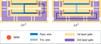
| 2 Encoding | Fermion-parity encoding (tetron) · primary ▣ Fig. 2 (single-qubit tetron gate schematic with measurement loops); §II.B Device design ✅ joint fermion parity of two Majorana wires (tetron); no X-direction measurement on Majorana 2; no machine-specific encoding source |
| 3 Gate mechanism | Measurement-based Majorana gate · primary ▣ Fig. 3 (measurement sequence = braid of MZMs 1,2); §III Measurement-based braiding transformations ✅ measurement-based braiding by parity-measurement sequences; node status X: no qubit, 2Q operation, braiding or gate demonstrated |
| 4 Connectivity / transport | Static nearest-neighbour lattice · primary ▣ Fig. 6 (gate schematic of 4×2 tetron array, columns joined by double-rail quantum dots); Fig. 4 🔎 tetron lattice — architectural intent; no multi-tetron device measured |
| 5 Control | Baseband electrical control (spins, Majorana) · primary ▤ §Device design and setup; Fig. 3 caption (VWP1 gate voltage and B∥ operating point) ✅ baseband gate voltages |
| 6 Readout | rf quantum-capacitance parity readout · primary ▣ Fig. 1 (TQDI dispersive gate-sensing loop); Fig. 3 (parity measurement A1); Fig. 4 (simulated CQ) ✅ rf quantum-capacitance interferometric parity readout: ~1% assignment error, SNR 1 in 3.6 µs; X lifetime ~1000× shorter than Z (2025); figures from Atlas ro_qcap, not this page |
| 7 Code | — (Atlas gap: ∅G-pathcode) · primary ▣ Fig. 7 (ZZ measurement circuit, ladder code); Fig. 9 (4.8.8 Hastings–Haah / 3-aux surface code); §IV ✅ empty L7 on topo architecture; MS 4D geometric codes [[96,6,8]] need all-to-all, not a tetron lattice; honeycomb_floquet is the natural fit and not on the topo architecture |
| 8 Decoder | |
| 9 Interconnect | |
| 10 Manufacturing | III-V MBE heterostructures (InAs–Pb wires, QD sources) · primary ▣ Fig. 2a (material-stack cross-section of the gate-defined superconducting nanowire) ✅ in-house III-V MBE heterostructure growth (InAs–Al); no external replication of the material stack; the 2026 InAs–Pb stack raises the superconductor's own gap (≈1.3 meV vs 295 µeV) and the induced gap (≈570 vs 129 µeV) about fourfold, the top-quintile topological gap only about twofold (~70 vs ~30 µeV) — arXiv:2606.03884; PRB 107, 245423 |
Standard records
SPAM error → 0.01 · best (parity assignment error)
single-wire parity only · Feb 2025 · source
evidence: ✅ 7 / 10
Pictures
Every picture carries the story of what it shows and its credit line.