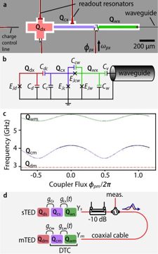
Toshiba double-transmon coupler
Toshiba + RIKEN RQC + University of Tokyo
Toshiba double-transmon coupler
פרופיל המרשם — הגרסה של המכונה לארכיטקטורה שלה (שדות המרשם באנגלית)
סוג הקיוביט: fixed-frequency transmon
מנגנון השער: double-transmon coupler (two transmons sharing a three-junction loop), external flux switches the interaction; CZ 48 ns
קישוריות: two-qubit test pair
בקרה: room-temperature RF; a shunt capacitance variant removes DC bias current at idle
מיקום הבקרה: room-temp
קריאה: dispersive
ראיה לשער: מאמר מדידה עם הפרוטוקול שלו
דגלים: רכיב, לא מכונה
טכנולוגיות לפי שכבה — התא של המכונה בכל שכבה
| 1 נושא הקיוביט | |
| 2 קידוד | קיוביט פיזי חשוף (ללא קידוד) · ראשית ◌ 🔎 Bare two-level subspace — Computational subspace of an anharmonic oscillator; leakage to |2⟩ is the price. |
| 3 מנגנון השער | CZ / iSWAP במצמד בר-כוונון · ראשית ▣ Fig. 1a (DTC circuit); §IV CZ-gate implementation; Fig. 4c-d (interleaved RB; 12-hour CZ-error run); Fig. 5 (error vs gate length) ✅ double-transmon coupler (two transmons, three-junction loop), flux-switched; CZ 99.90% averaged over 12 h at 48 ns; residual ZZ ≈6 kHz off (Nov 2024) |
| 4 קישוריות והובלה | סריג סטטי של שכנים קרובים · ראשית ▣ Fig. 1b (false-color picture of the two-qubit device: Q1-Q2 joined by the DTC) ✅ two-qubit test pair (degree 1); no multi-qubit DTC processor exists |
| 5 בקרה | אלקטרוניקה בטמפרטורת החדר + כבל קואקסיאלי/כבל גמיש לכל קיוביט · ראשית ▣ Fig. 6 (schematic diagram of the measurement setup); Appendix B Measurement setup; Fig. 2 (Z-pulse on coupler loop) ✅ room-temperature RF with external flux bias; shunt-capacitance variant idles at zero flux, no DC bias current (PRApplied 23, 064069, Jun 2025) |
| 6 קריאה | קריאה דיספרסיבית במיקרוגל (+TWPA, מסנן פרסל) · ראשית ▣ Fig. 1a (readout elements); Fig. 10 (single-shot readouts of the three resonators); Appendix F State discrimination ✅ dispersive |
| 7 קוד | |
| 8 מפענח | |
| 9 חיבור בין-מודולי | |
| 10 ייצור | ליתוגרפיה של קיוביטים מוליכי-על (צמתי Al/AlOx/Al, חיווט Nb, 300 mm) · ראשית ▤ Appendix A: Fabrication ✅ |
רשומות סטנדרטיות
הפרעה הדדית → 6.0e+3 Hz · best published for superconducting (residual ZZ in the off state)
Nov 2024 · מקור
שגיאת 2Q בפעולה מקבילית על כל הרוחב → 1.00e-3 · best-of-line (99.90% CZ averaged over 12 h on a 2-qubit device)
Nov 2024 · מקור
רלקסציית T1 → 230 µs · הטוב ביותר
Nov 2024 · מקור
קוהרנטיות T2 (הד/DD) → 360 µs · הטוב ביותר
Nov 2024 · מקור
ראיות: ✅ 6 / 10
תמונות
כל תמונה מלווה בתיאור של מה שהיא מראה ובשורת הקרדיט שלה.